Domain crossing device

a domain crossing and domain technology, applied in the field of semiconductor devices, can solve the problems of invalid pulse of selection signal selb, delay phase detection period signal fpvt_detd, and cannot be used in the above-mentioned method of single clock domain crossing, etc., to achieve the effect of stably performing a domain crossing operation

Active Publication Date: 2008-03-04
SK HYNIX INC
View PDF7 Cites 40 Cited by
  • Summary
  • Abstract
  • Description
  • Claims
  • Application Information

AI Technical Summary

Benefits of technology

[0073]It is, therefore, an object of the present invention to provide a domain crossing device capable of stably performing a domain crossing operation regardless of variations of process, voltage and temperature.

Problems solved by technology

Therefore, the above-mentioned method of the single clock domain crossing cannot be used in this case.
The second problem PROBLEM2 is that the selection signal selB has an invalid pulse.
The third problem PROBLEM3 is that the delayed phase detection period signal fpvt_detd is not in a valid period ((A) to (B)) of the detection starting signal startz.
The fourth problem PROBLEM4 is that the termination unit 21D may output an unintended signal when the selection signal selB is changed.
Therefore, even if initial states are changed due to variations of process, voltage and temperature (PVT), the change cannot be applied.
Therefore, due to the above-mentioned problems of the conventional domain crossing device, a data may not be synchronized with an external clock signal when the data is outputted from a semiconductor memory device.
As a result, a reliability of the semiconductor memory device is degraded.

Method used


Image

  • Domain crossing device
  • Domain crossing device
  • Domain crossing device

Examples


Embodiment Construction

[0105]Hereinafter, a domain crossing device in accordance with the present invention will be described in detail referring to the accompanying drawings.

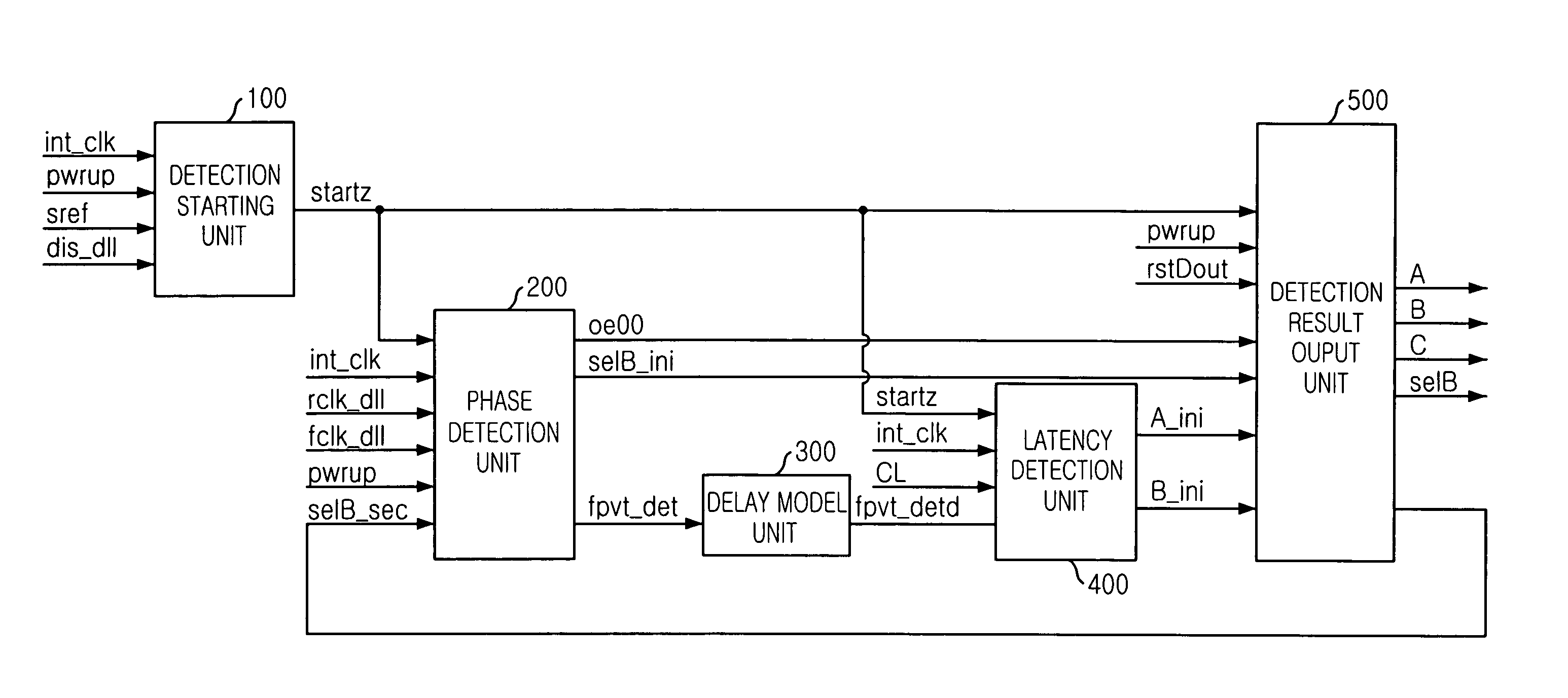
[0106]FIG. 10 is a block diagram showing a domain crossing device in accordance with a preferred embodiment of the present invention.

[0107]As shown, the domain crossing device includes a detection starting unit 100, a phase detection unit 200, a delay model unit 300, a latency detection unit 400 and a detection result output unit 500.

[0108]The detection starting unit 100 generates a detection starting signal startz so that the latency detection unit 400 and the detection result output unit 500 can be operated.

[0109]The phase detection unit 200 detects phases of a rising edge DLL clock signal rclk_dll and a falling edge DLL clock signal fclk_dll comparing the phases of the rising and falling edge DLL clock signals rclk_dll and fclk_dll with a phase of an internal clock signal int_clk.

[0110]The delay model unit 300 compensates a flight...


PUM


Abstract

A domain crossing device for use in a semiconductor memory device, including: a unit for comparing a phase of an internal clock signal with a phase of a delay locked loop (DLL) clock signal to generate a first clock selection signal and a phase detection period signal in response to a detection starting signal and a second clock selection signal; a unit for generating a plurality of initial latency signals in response to the phase detection period signal, the detection starting signal and a column address strobe (CAS) latency signal; a unit for receiving the plurality of initial latency signals and the detection starting signal to generate a plurality of latency signals, a clock selection signal and the second clock selection signal; and a unit for generating the detection starting signal based on a self refresh signal, a power-up signal and a DLL disable signal.

Description

FIELD OF INVENTION[0001]The present invention relates to a semiconductor device; and, more particularly, to a domain crossing device for use in a semiconductor memory device.DESCRIPTION OF PRIOR ART[0002]Generally, a semiconductor memory device includes more than one clock domain. That is, a data-receiving block of the semiconductor memory device is operated in synchronization with a first clock signal, whereas a data-transmitting block of the semiconductor memory device is operated in synchronization with a second clock signal. An interface between clock domains is called a domain crossing where signals cross a boundary of the clock domains.[0003]FIG. 1 is a block diagram showing a conventional semiconductor memory device including a domain crossing device.[0004]As shown, the conventional semiconductor memory device includes a first clock domain block 100 and a second clock domain block 200. The first clock domain block 100 uses an internal clock signal int_clk for a reference cloc...

Claims


Application Information

Patent Timeline
Patent Type & Authority Patents(United States)
IPC IPC(8): G06F1/04G06F1/12G11C7/22G11C8/00G11C8/18
CPCG11C7/22G11C8/18G11C7/222
Inventor PARK, NAK-KYU
Owner SK HYNIX INC
Why Eureka
Try Eureka