Split socket optical interconnect

a technology of optical interconnection and socket, which is applied in the field of sockets, can solve the problems of electrical interconnections having limitations, power consumption continuing to rise, and socket requirements becoming more challenging

Inactive Publication Date: 2008-03-18
INTEL CORP
View PDF22 Cites 34 Cited by
  • Summary
  • Abstract
  • Description
  • Claims
  • Application Information

AI Technical Summary

Problems solved by technology

As microprocessor speeds have continued to increase, socket requirements are becoming more challenging.
Power consumption continues to trend upward, driven by the increased leakage current of smaller silicon features, the increased dynamic current required to scale frequency, and the incorporation of multiple cores within a single package.
Electrical interconnects may have their limitations.
For example, currently planned electrical implementations of the common system interface (CSI) protocol links may be limited in the bandwidth distance product even at 6.4 gigabits / second (Gb / s).

Method used


Image

  • Split socket optical interconnect
  • Split socket optical interconnect
  • Split socket optical interconnect

Examples


Embodiment Construction

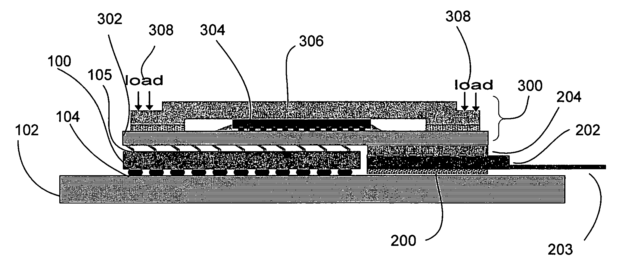
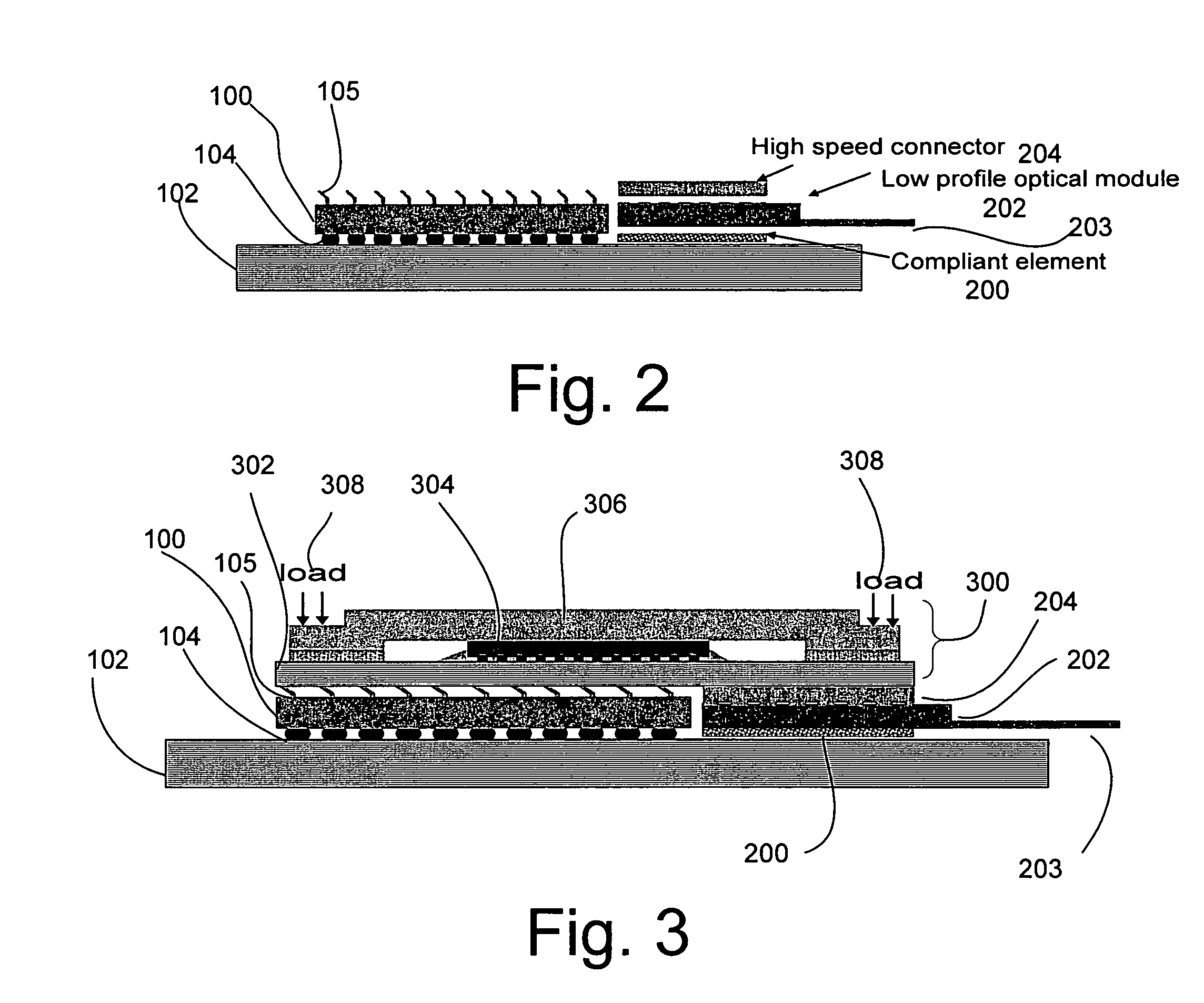
[0013]A low cost optical interconnect, closely packaged with the microprocessor, may alleviate electrical system constraints due to the improved channel bandwidth provided by optical interconnects. A split socket is disclosed that provides at least one cavity created at an outer edge of the microprocessor socket. An optical module may be fitted in the cavity thus providing an optical fiber or waveguide connection directly to the socket.

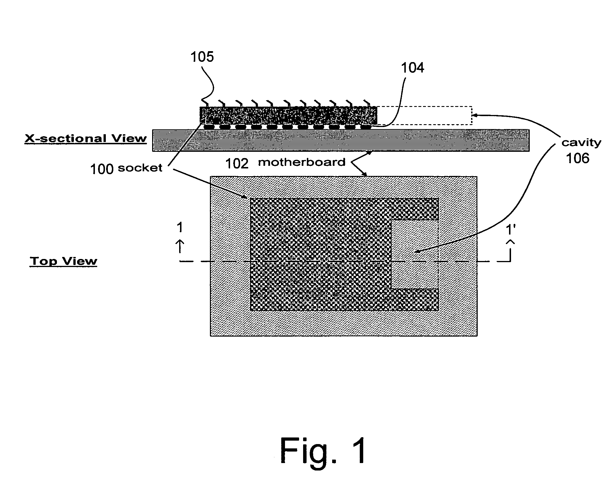
[0014]Referring now to FIG. 1, there is shown a top view and a cross-sectional view taken along line 1-1′ of a socket according to embodiments of the invention. A socket 100 is mounted to a motherboard 102. Electrical and / or mechanical connections may be provided between the two by solder balls 104 or any suitable method. Pins 105 may be provided for later connection with a microprocessor package. A cavity 106 may be formed at one edge of the socket 100. The cavity 106 may be sized to accommodate, for example, an optical module. The cavity 106 is illu...


PUM


Abstract

A split microprocessor socket is disclosed that provides a cavity created at an outer edge of the microprocessor socket. An optical module may be fitted in the cavity thus providing an optical fiber or waveguide connection directly to the socket. This low cost optical interconnect, closely packaged with the microprocessor, may alleviate bandwidth constraints associated with conventional electrical connections.

Description

FIELD OF THE INVENTION[0001]Embodiments of the present invention relate to sockets and, more particularly, to microprocessor sockets having an optical interconnect.BACKGROUND INFORMATION[0002]Since the introduction of the Personal Computer (PC), the microprocessor has interfaced with the system motherboard through a socket. The role of the socket is to provide electrical connectivity between the microprocessor and the motherboard, while also allowing tool-free installation, removal and interchangeability of the microprocessor without damage.[0003]As microprocessor speeds have continued to increase, socket requirements are becoming more challenging. Power consumption continues to trend upward, driven by the increased leakage current of smaller silicon features, the increased dynamic current required to scale frequency, and the incorporation of multiple cores within a single package. At the same time, the required socket bandwidth to support the necessary high-speed signaling is also ...

Claims


Application Information

Patent Timeline
Patent Type & Authority Patents(United States)
IPC IPC(8): H01R12/00
CPCG02B6/4201G02B6/4214H01L2224/73253H01L2224/73204G02B6/4249G02B6/4284
Inventor LU, DAOQIANGALDUINO, ANDREW C.BRAUNISCH, HENNING
Owner INTEL CORP
Why Eureka
Try Eureka