
Method and apparatus for high voltage operation for a high performance semiconductor memory device

Active Publication Date: 2008-03-18
INFINEON TECH LLC
View PDF8 Cites 30 Cited by
  • Summary
  • Abstract
  • Description
  • Claims
  • Application Information

AI Technical Summary

Benefits of technology

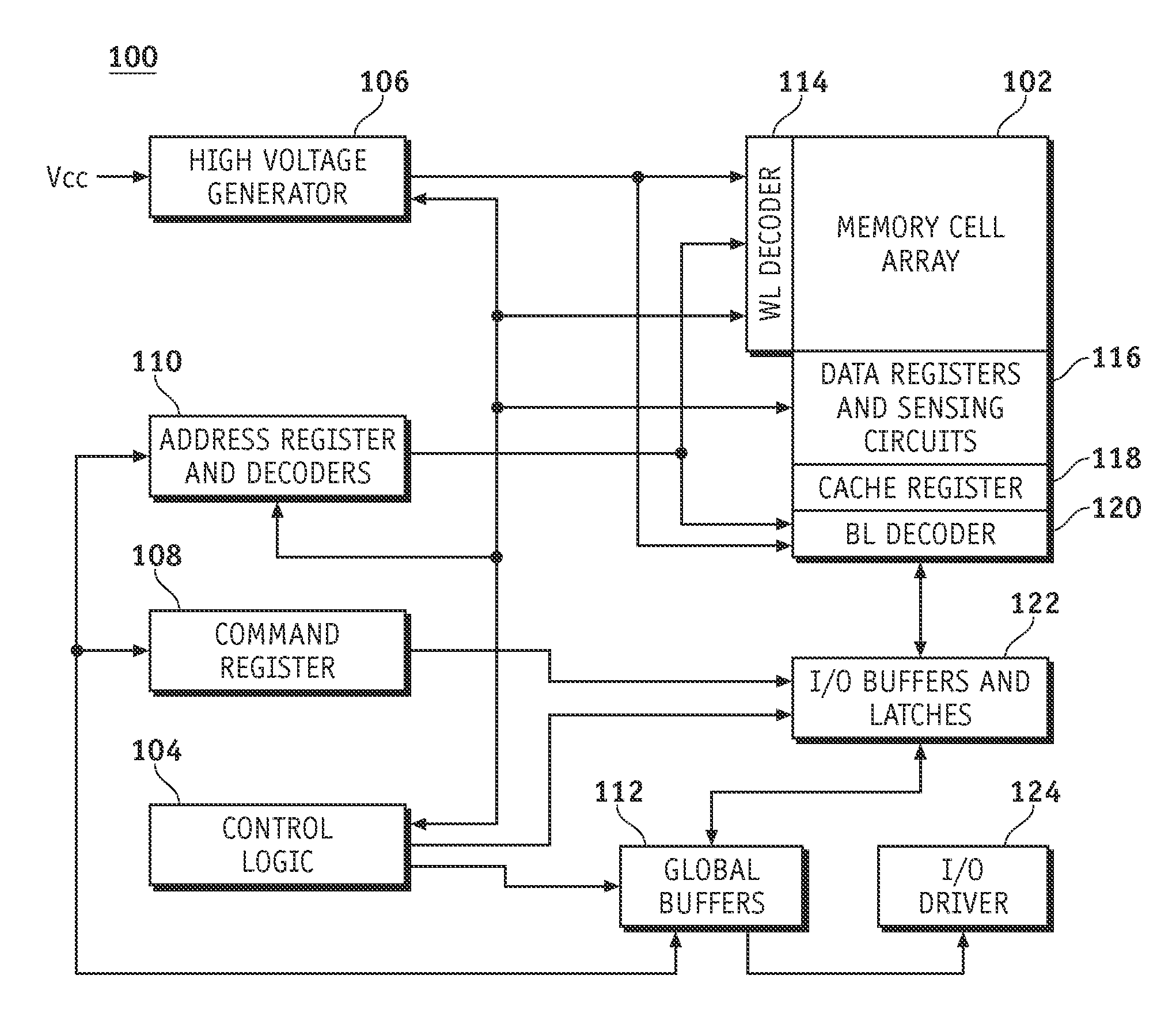
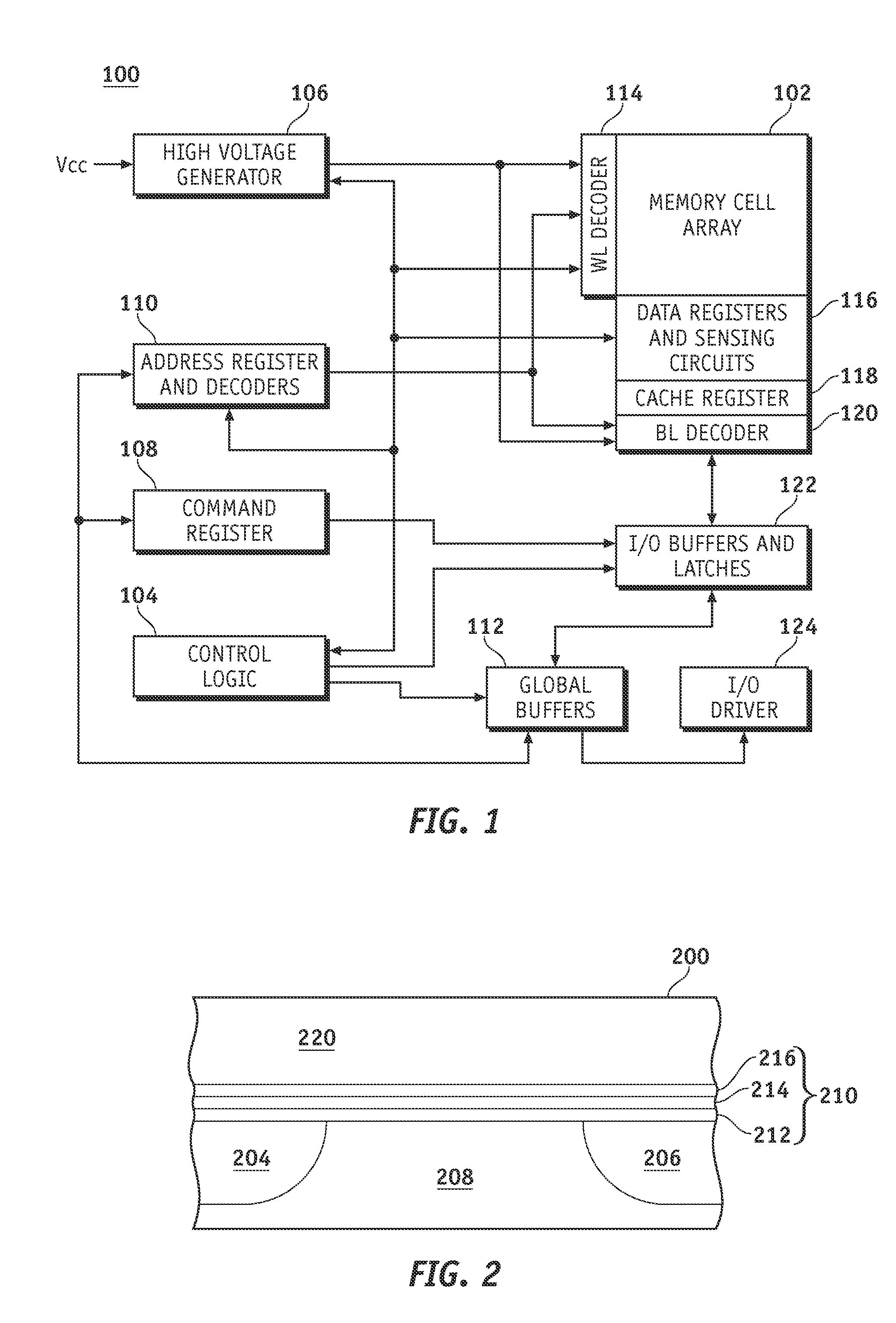
[0007]In accordance with an additional aspect of the present invention, the high voltage generator provides the high voltage level to a first and a second high voltage node and includes a current flow control device to decouple the first high voltage node from the second high voltage node. A word line decoder is coupled to the first high voltage node and provides the high voltage level from the first high voltage node to selected word lines for programming of the selected memory cells and a bit line decoder is coupled to the second high voltage node and selectively connects the second high voltage node to selected bit lines to provide the high voltage level to the selected memory cells for programming thereof. The bit line decoder provides a boosting voltage from the high voltage generator to the selected bit lines at a predetermined time to overcome a voltage level drop resulting from the capacitor load associated with the selected bit lines.

Problems solved by technology

Thus, the drain pumps take time to ramp up to a targeted high voltage level.
Given the ramping limitations of conventional high voltage generating devices, it is difficult for many semiconductor memory devices to provide erase, program and read operations of sufficient speed to operate as NAND-type memories.

Method used


Image

  • Method and apparatus for high voltage operation for a high performance semiconductor memory device
  • Method and apparatus for high voltage operation for a high performance semiconductor memory device
  • Method and apparatus for high voltage operation for a high performance semiconductor memory device

Examples


first embodiment

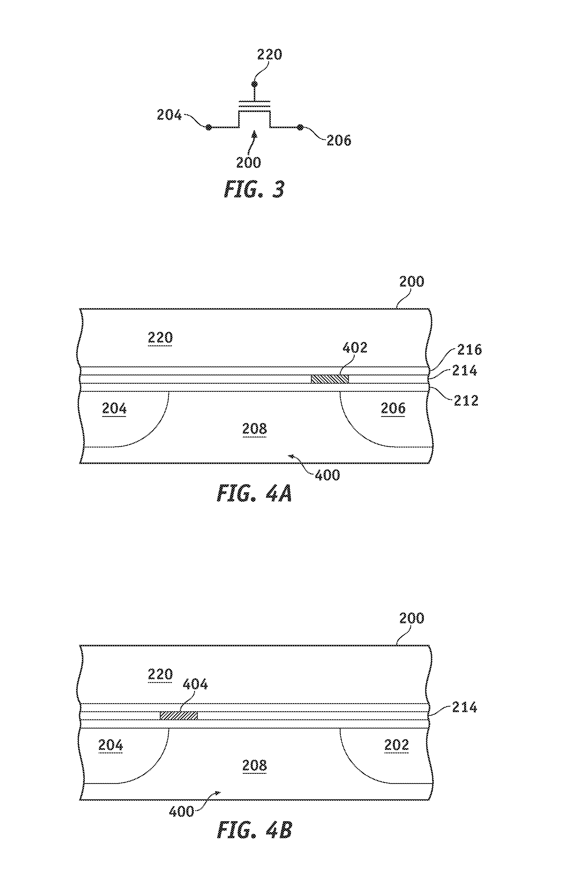
[0039]Referring to FIG. 4, consisting of FIGS. 4A and 4B, an erase operation on the two-bit memory cell of FIG. 2 in accordance with the present invention is depicted wherein FIG. 4A depicts erasing a first, or right, bit 402 of the two-bit memory cell 200 and FIG. 4B depicts erasing a second, or left, bit 404 of the two-bit memory cell 200. The high voltage erase operation uses band-to-band hot hole injection into the nitride layer to neutralize the electrons trapped therein.

[0040]Referring to FIG. 4A, the first bit 402 is erased by providing a high voltage level of −6 volts to the word line 220 and +4 volts to the drain 206; the open end (i.e., the source 204) remains floating. In this manner, the hot holes 410 are injected from the drain 206 into the channel 208 and the first bit 402 formed in a localized region above the portion of the channel 208 adjoining the drain 206, thereby neutralizing the electrons stored in the first bit 402.

[0041]Referring to FIG. 4B, the second bit 40...

second embodiment

[0057]Referring to FIG. 12, high voltage drain pumps 1202 in accordance with the present invention provide a first high voltage node 1204 coupled to the word line 502 and a second high voltage node 1206 coupled to the gates of the bit line decoder pass transistors 902 for programming of memory cells 200. A current flow control device 1204, such as a diode, is provided in the drain pumps 1202 to decouple the first high voltage node 1204 from the second high voltage node 1206. As the first and second high voltage nodes 1204, 1206 are decoupled, a higher voltage level (e.g., 10 volts) can be applied to the second high voltage node 1206 than the voltage level (e.g., 9.5 volts) applied to the first high voltage node 1204.

[0058]In addition, a boosting voltage is provided to the second high voltage node 1206 to hasten recovery from the voltage level drop resulting from the capacitor load associated with the switching of the bit lines 504. The timing of the boosting voltage is controlled by...

third embodiment

[0064]In accordance with the present invention, however, an improved method for high voltage programming of selected memory cells 200 is provided which increases the speed of high voltage programming while conserving power expended in the programming. The improved method includes the steps of providing a high voltage level to data blocks 1514 associated with a first portion of the bit lines 504 for a predetermined time interval to program a first portion of the selected memory cells 200, precharging a second portion of the bit lines 504 during the predetermined time interval that the high voltage level is provided to the data blocks 1514 and, thereafter, providing the high voltage level to data blocks 1514 associated with the second portion of the bit lines 504 for the predetermined time interval to program a second portion of the selected memory cells. During both the first and second predetermined time intervals, a continuous high voltage level is provided to selected word lines 5...


PUM


Abstract

A method and apparatus are provided for high performance, high voltage memory operations on selected memory cells (200) of a semiconductor memory device (100). A high voltage generator (106) during program or erase operations provides a continuous high voltage level (702) on selected word lines (502) and maintains a continuous high voltage level supply to a bit line decoder (120) which sequentially provides the high voltage level (706) to a first portion of bit lines (504) and discharges (708) those bit lines (504) before providing the high voltage level to a second portion (710).For additional improvements to program operations, the high voltage generator (106) decouples high voltages provided to the word lines (502) and the bit lines (504) by providing a current flow control device (1208) therebetween and provides a boosting voltage at a time (1104) to overcome a voltage level drop (1102) resulting from a capacitor load associated with selected bit lines (504) and / or the bit line decoder (120) precharges (1716) a second portion of the bit lines (504) while providing a high voltage level to a first portion to program (1706) a first portion of memory cells (200).For improvements to read operations, whether dynamic reference cells (2002) are blank is determined by providing non-identically regulated high voltage levels from a first voltage source (2112) to the dynamic reference cells (2002) and from a second voltage source (2104) to static reference cells (2004) and, if the dynamic reference cells (2002) are not blank, reads selected memory cells (200) by providing identically regulated high voltage levels to the selected memory cells (200), the dynamic reference cells (2002) and the static reference cells (2004).

Description

FIELD OF THE INVENTION[0001]The present invention generally relates to semiconductor memory devices, and more particularly relates to a method and apparatus for high voltage operation in a nonvolatile memory device.BACKGROUND OF THE INVENTION[0002]Semiconductor memory devices typically include a memory cell array wherein a particular memory cell is erased, programmed or read by providing appropriate voltages to word lines via an word line decoder and bit lines via a bit line decoder. In semiconductor memory devices, such as flash memory devices utilizing a single bit or multi-bit memory cell having an insulative charge trapping layer for storing information, high voltage is required to erase, program or read such information from or into the memory cell. Drain pumps and similar high voltage generating circuits are utilized to provide high voltage and / or high current for such semiconductor memory operation. For example, in such semiconductor memory devices, drain pumps are used to pr...

Claims


Application Information

Patent Timeline
IPC IPC(8): G11C16/04G11C16/06G11C5/14G11C7/00
CPCG11C7/1039G11C8/08G11C16/08G11C16/30G11C16/0475G11C16/0491G11C2207/2245
Inventor YANG, NIANANG, BOON-AIKWU, YONGGANGWANG, GUOWEILAI, FAN WAN
Owner INFINEON TECH LLC
Learn More