Automatic built-in self-test of logic with seeding from on-chip memory

Active Publication Date: 2008-03-18
MONTEREY RES LLC
View PDF13 Cites 19 Cited by
  • Summary
  • Abstract
  • Description
  • Claims
  • Application Information

AI Technical Summary

Benefits of technology

[0023]Such an arrangement can allow for an integrated circuit device to include multiple seed values that are rapidly available for BIST operations. In this way, a device may include a self-contained set of seed values for a high degree of test coverage. This can dispense with the need for expensive automatic test equipment (ATE) that sequentially loads seed values into a device.
[0024]According to one aspect of the embodiments, a test pattern generator can include a linear feedback shift register. Such an arrangement can allow for rapid generation of test patterns from seed values provided by a seed value memory.
[0025]According

Problems solved by technology

Unfortunately, such an approach is typically only possible for relatively simple devices, as conventional BIST circuits for more complex device do not provide sufficient test “coverage”.
That is, a self-test may not be thorough enough, or test enough features/combinations of a device to adequately determine the location and/or type of defect.
However, even with very expensive high speed testers, such an approach may take considerable time and/or not apply such values at the clock speed (e.g., normal operating speed) of the integrated circuit.
While a conventional auto-BIST approach like that of FIG. 10 may be sufficient for simple devices, such an approach may not be adequate or fast enough for more complex devices.
In particular, self-testing f

Method used


Image

  • Automatic built-in self-test of logic with seeding from on-chip memory
  • Automatic built-in self-test of logic with seeding from on-chip memory
  • Automatic built-in self-test of logic with seeding from on-chip memory

Examples


first embodiment

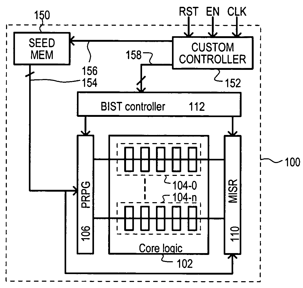
[0053]Referring now to FIG. 1, a BIST section is set forth in a block schematic diagram and designated by the general reference character 100. A BIST section 100 can include a tested section 102, a test pattern generator 106, a result output circuit 110, and a test controller 112. In addition, and unlike conventional BIST arrangements, a BIST section 100 can also include a seed value memory 150 and seed selector circuit 152.

[0054]In one very particular arrangement, a tested section 102 can include a core logic portion. A tested section 102 can be self-tested by way of one or more scan chains (104-0 to 104-n) coupled to and / or incorporated into tested section 102.

[0055]A test pattern generator 106 can generate multiple test patterns in response to a single seed value. A test pattern generator 106 can preferably include a pseudo-random pattern generator (PRPG), more preferably a PRPG that includes a linear feedback shift register (LFSR).

[0056]A result output circuit 110 can preferabl...

second embodiment

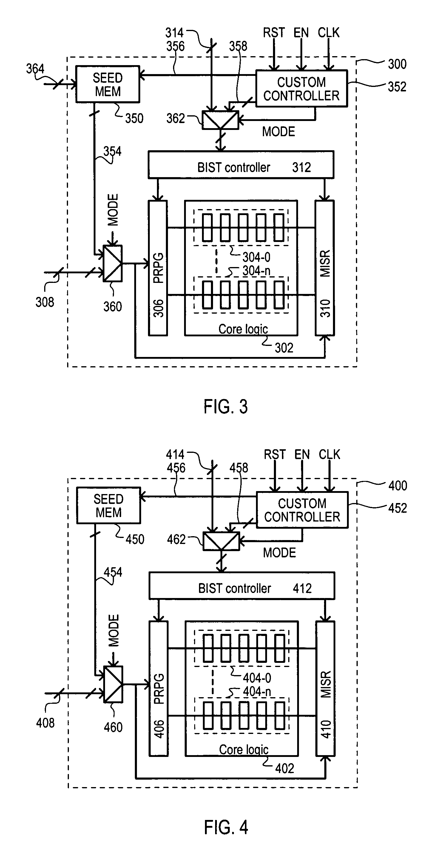
[0065]Referring now to FIG. 3, a BIST section is set forth in a block diagram and designated by the general reference character 300. A BIST section 300 can include some of the same items as FIG. 1. Accordingly, like items will be referred to by the same reference character but with the first digit being a “3” instead of a “1”.

[0066]The embodiment of FIG. 3 can differ from that of FIG. 1 in that BIST data and / or control values may be loaded via separate inputs. Such an arrangement can allow for BIST operations to occur by way of seed values already present within an onboard seed memory, or according to seed values received externally on a test input. Thus, the embodiment of FIG. 3 can include a test input 308, a test control input 314, a seed multiplexer 360, a control multiplexer 362, and a memory input 364.

[0067]A seed multiplexer 360 can operate according to a mode value MODE, and enable a seed value to be applied to a test pattern generator 306 from a seed value memory 350 or fro...

third embodiment

[0072]Referring now to FIG. 4, a BIST section is set forth in a block diagram and designated by the general reference character 400. A BIST section 400 can include the same essential items as FIG. 3. Accordingly, like items will be referred to by the same reference character but with the first digit being a “4” instead of a “3”.

[0073]The embodiment of FIG. 4 can differ from that of FIG. 3, in that a seed value memory can be fabricated or otherwise manufactured to include seed values (e.g., mask ROM, fuse-type structures). As such, a memory input (e.g., 364 of FIG. 3) may not be included. This can allow for smaller pin counts and / or fewer signal lines than the embodiment of FIG. 3.

[0074]Having described the structure of various embodiments of the present invention, another method according to an embodiment will now be described with reference to FIG. 5.

[0075]Referring to FIG. 5, a method 500 can include establishing seed values in an onboard memory (step 502). A step 502 can include,...


PUM


Abstract

Built-in self-test (BIST) devices and methods are disclosed. A BIST section (100) according to one embodiment can include a built-in seed value memory (150) that stores multiple seed values. In a BIST operation, a seed value can be transferred from a built-in seed memory (150) to a test pattern generator (106) to generate multiple test patterns for scan chains (104-0 to 104-n). Successive seed values can be transferred to generate multiple test patterns sets at a clock speed and/or to achieve a desired test coverage.

Description

TECHNICAL FIELD[0001]The present invention relates generally to the self-testing of integrated circuits, and more particularly to integrated circuits having a built-in self-test (BIST) capability.BACKGROUND OF THE INVENTION[0002]The testing of integrated circuits can occur throughout the life of a device. An integrated circuit may be tested in die form, while still part of a wafer, in packaged form at the “back” end of a manufacturing process, and / or after the device has been incorporated into a system (“in system” testing).[0003]Self-test can increase the speed at which a device is tested, as an integrated circuit can typically operate at a faster speed than a tester. Moreover, built-in self-test (BIST) circuits can incorporate more complex test functions on the device itself, which can reduce or eliminate the need for expensive complex tester equipment.[0004]While self-test can perform an important function in screening new devices, self-test can also perform an important function...

Claims


Application Information

Patent Timeline
IPC IPC(8): G01R31/28
CPCG01R31/318547G01R31/318555
Inventor MAHESHWARI, DINESHWRIGHT, ANDREW
Owner MONTEREY RES LLC
Why Eureka
Try Eureka