System, method and computer program product for designing connecting terminals of semiconductor device

a technology of connecting terminals and computer programs, applied in the direction of cad circuit design, program control, instruments, etc., can solve the problems of insufficiently satisfying design requirements, high probability of differential buffer cells not being arranged at adjacent i/o slots, and affecting the design effect of the device,

Inactive Publication Date: 2008-04-01
KK TOSHIBA
View PDF4 Cites 14 Cited by
  • Summary
  • Abstract
  • Description
  • Claims
  • Application Information

AI Technical Summary

Problems solved by technology

When designing connecting terminals, however, these packages have some technical problems due to the structures thereof being different from those of the QFPs.
Further, there is a high probability of differential buffer cells not being arranged at adjacent I / O slots.
Design requirements concerning, for example, equal-length wires and pair wires needed by cell specifications are insufficiently satisfied in the BGA.
This, however, results in increasing the number of wiring intersections in each connecting net, thus making detailed wiring designing difficult.

Method used


Image

  • System, method and computer program product for designing connecting terminals of semiconductor device
  • System, method and computer program product for designing connecting terminals of semiconductor device
  • System, method and computer program product for designing connecting terminals of semiconductor device

Examples


Embodiment Construction

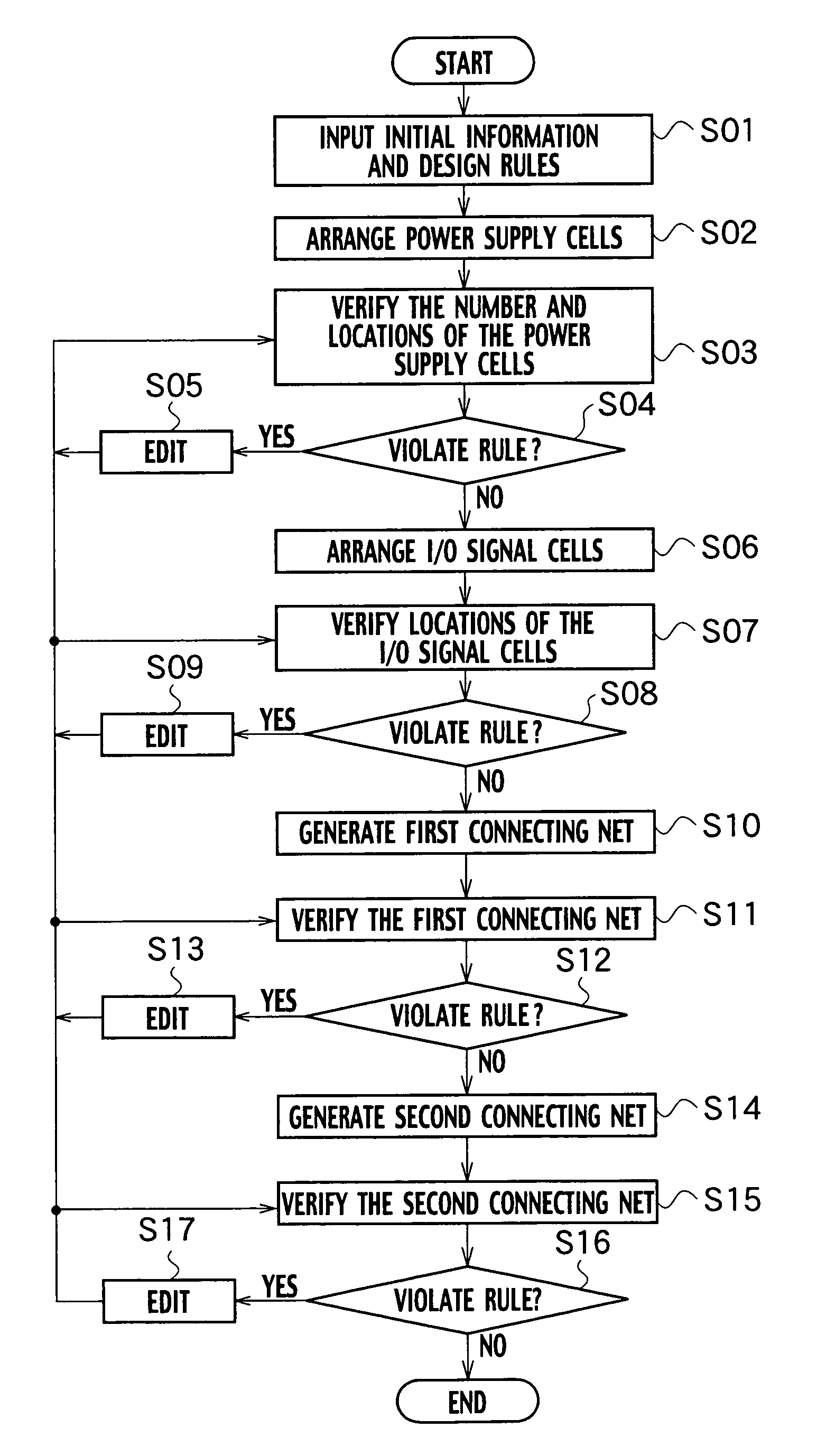
[0027]Various embodiments of the present invention will be described with reference to the accompanying drawings. It is to be noted that the same or similar reference numerals are applied to the same or similar parts and elements throughout the drawings, and the description of the same or similar parts and elements will be omitted or simplified.

[0028]Generally and as it is conventional in the representation of semiconductor devices, it will be appreciated that the various drawings are not drawn to scale from one figure to another nor inside a given figure, and in particular that the layer thicknesses are arbitrarily drawn for facilitating the reading of the drawings.

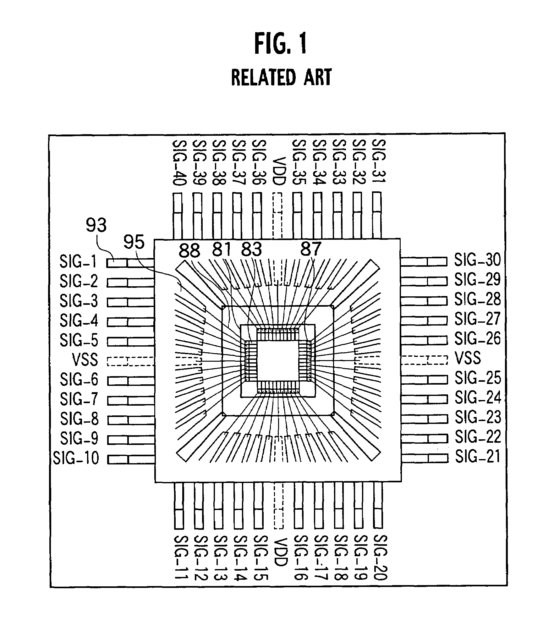
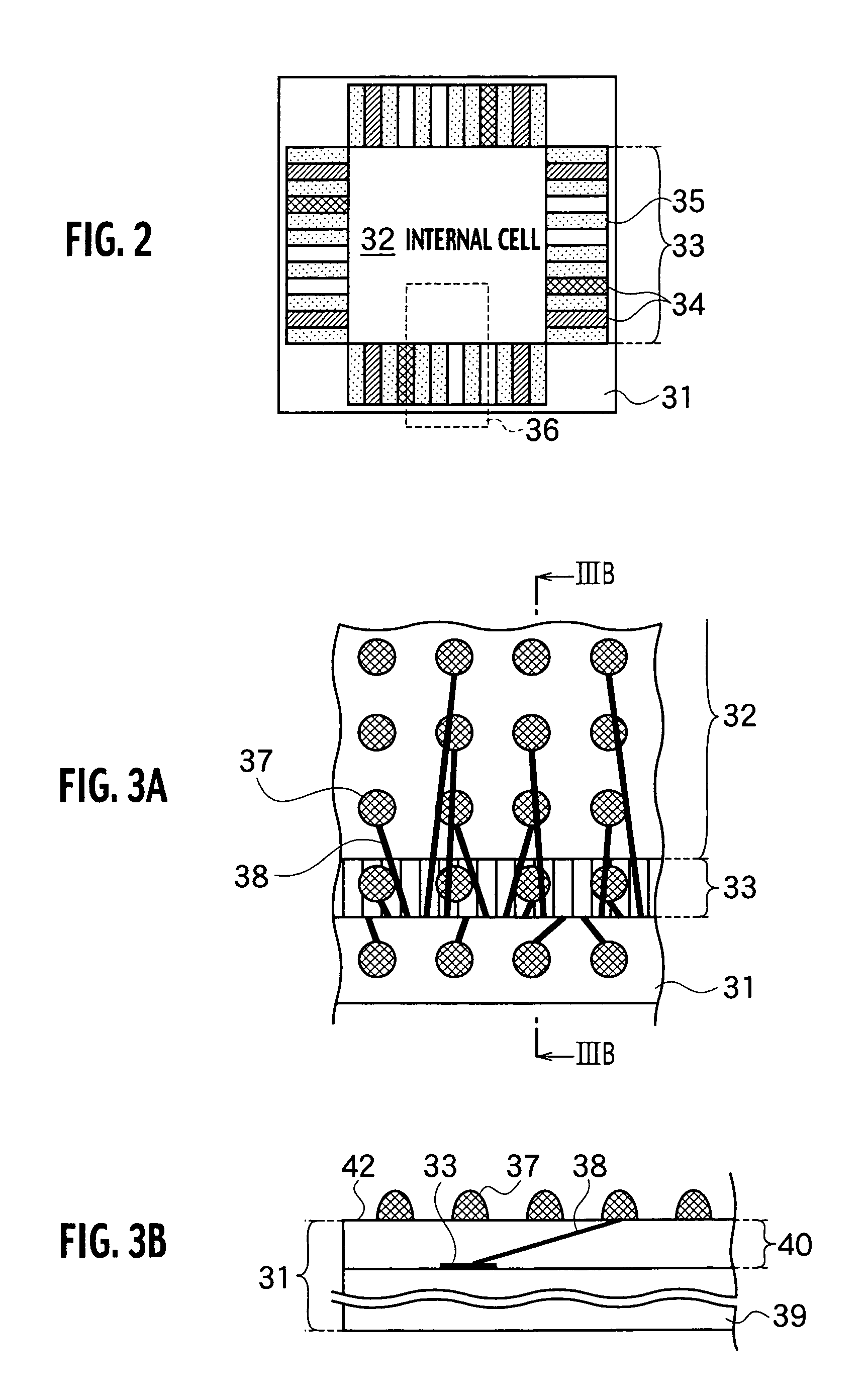
[0029]Before explaining the designing of connecting terminals of a semiconductor device according to embodiments of the present invention, a semiconductor device packaged in a flip-chip BGA for which connecting terminals are designed according to the embodiments will be explained.

[0030]FIG. 2 is a plan view generally sho...


PUM


Abstract

A system for designing connecting terminals of a semiconductor device, having a power supply cell arranging unit configured to arrange power supply cells at some of I / O slots formed in a semiconductor chip, an I / O signal cell arranging unit configured to arrange I / O signal cells at some of the I / O slots where the power supply cells are not arranged, a first connecting net generator configured to generate a first connecting net connecting the I / O slots to bumps formed on the semiconductor chip, a second connecting net generator configured to generate a second connecting net connecting the bumps to external electrodes formed on a package base, and a verifier configured to verify whether the power supply cells, I / O signal cells, and first and second connecting nets violate predetermined design rules.

Description

CROSS REFERENCE TO RELATED APPLICATIONS[0001]This application is based upon and claims the benefit of priority from the prior Japanese Patent Application No. P2002-204776 filed on Jul. 12, 2002; the entire contents of which are incorporated herein by reference.BACKGROUND OF THE INVENTION[0002]1. Field of the Invention[0003]The present invention relates to a system, method, and computer program product for designing connecting terminals of a semiconductor device, and particularly, to a pin assign process carried out before an automatic chip arranging / wiring process and a detailed package designing process in a semiconductor design flow.[0004]2. Description of Related Art[0005]FIG. 1 shows a quad flat package (QFP) according to a related art. The package includes package pins 93 arranged along the periphery of the package and inner lead pins 95 arranged inside the package and connected to a semiconductor chip 81. The pins 93 and 95 linearly run on the periphery of the package, and the...

Claims


Application Information

Patent Timeline
Patent Type & Authority Patents(United States)
IPC IPC(8): G06F17/50H01L21/82H01L21/822H01L23/12H01L27/04
CPCG06F17/5068G06F17/5072H01L23/50H01L2224/16225G06F30/392G06F30/39
Inventor IMADA, TOMOHIKOWATANABE, SEIJISHIBATA, TOYOKAZU
Owner KK TOSHIBA
Why Eureka
Try Eureka