Photonic crystal optical circuit and method for controlling the same

a technology of optical circuit and photonic crystal, which is applied in the direction of optical elements, cladded optical fibres, instruments, etc., can solve the problems of the optical circuit to be displayed, and achieve the effect of increasing the light receiving efficiency of the devi

Inactive Publication Date: 2008-04-15
NEC CORP
View PDF12 Cites 5 Cited by
  • Summary
  • Abstract
  • Description
  • Claims
  • Application Information

AI Technical Summary

Benefits of technology

[0025]As for the light receiving device, the direction of light reception by the light receiving device needs to be controlled in order to increase the light receiving efficiency of the device.

Problems solved by technology

However, if the functions of light emitting or light receiving devices are built into an optical circuit, these devices, simply arranged in the optical circuit, are unable to cause the function of the optical circuit to be displayed.

Method used


Image

  • Photonic crystal optical circuit and method for controlling the same
  • Photonic crystal optical circuit and method for controlling the same
  • Photonic crystal optical circuit and method for controlling the same

Examples


Embodiment Construction

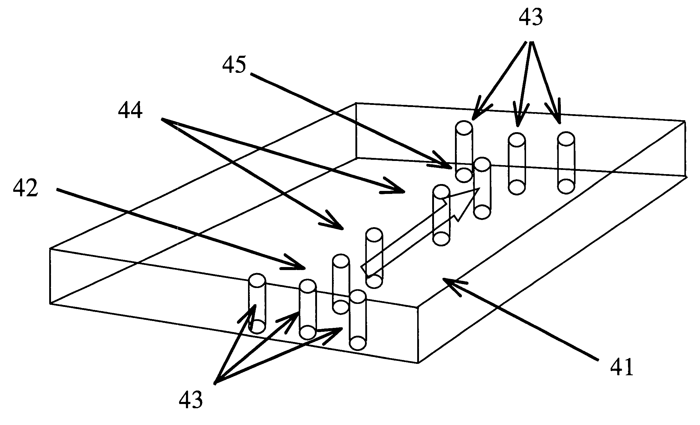
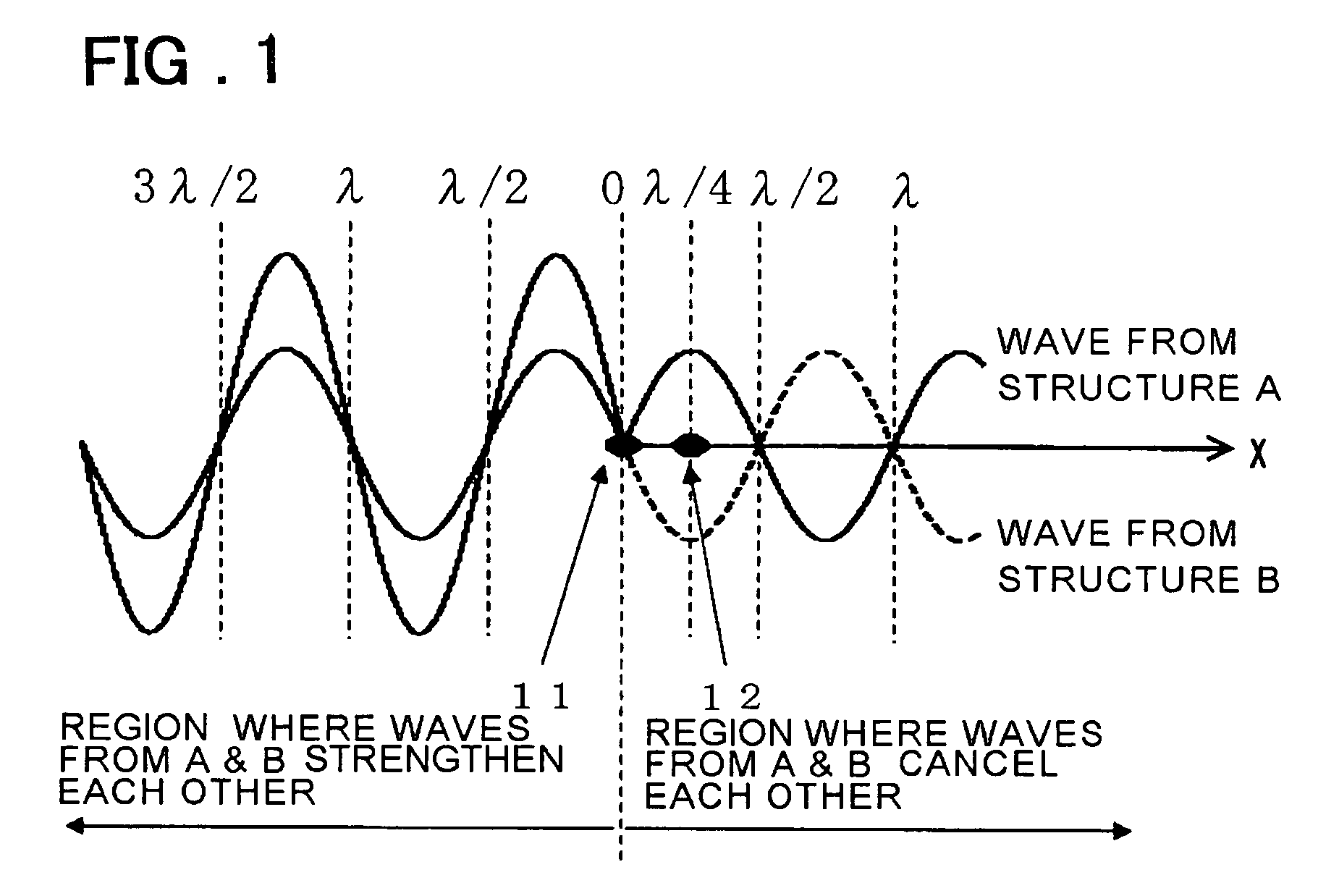
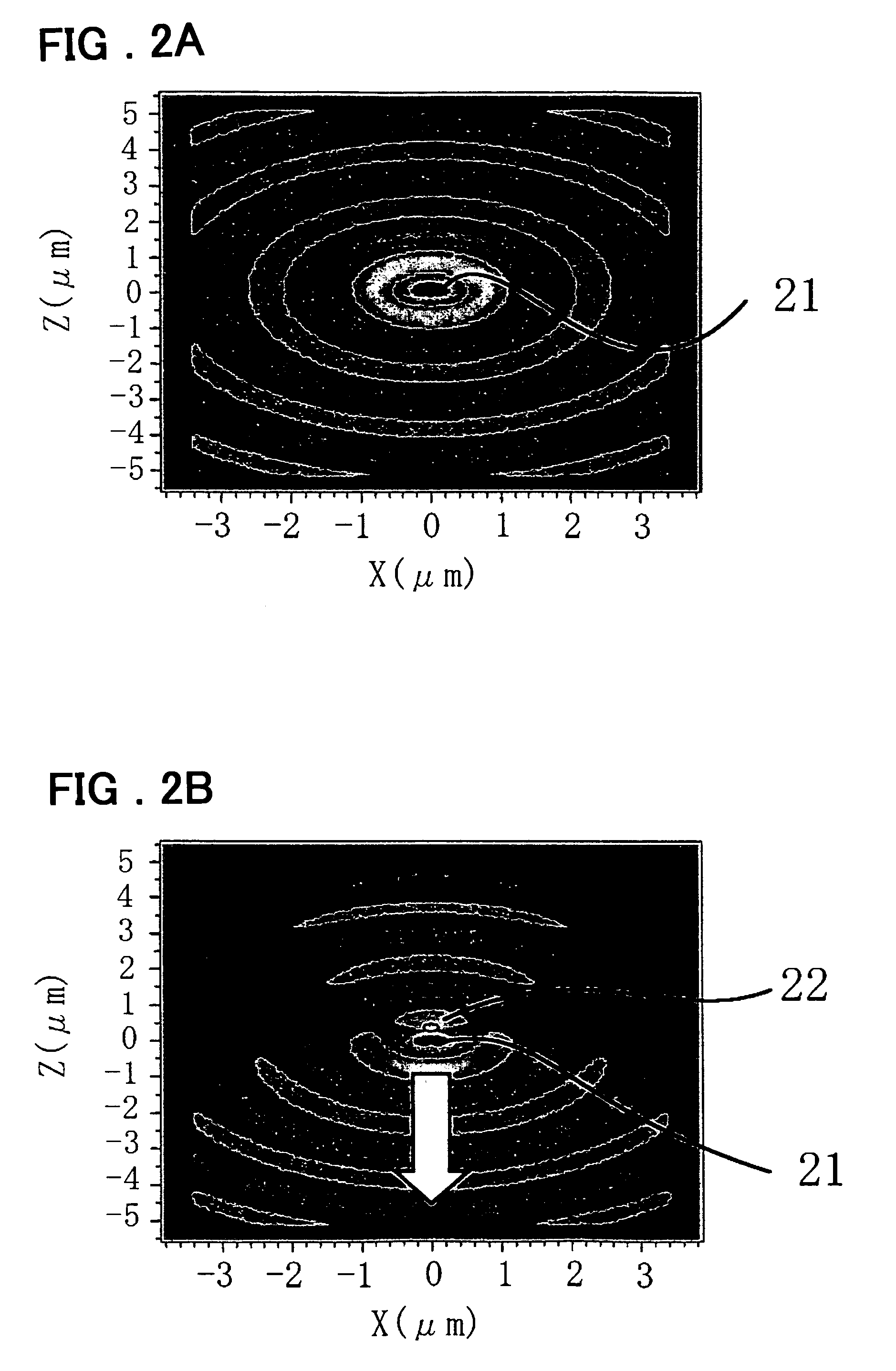
[0045]For more detailed explanation of the present invention, reference is made to the accompanying drawings. First, the principle of the present invention is explained, and preferred embodiments thereof will then be explained. With the above-described conventional technique of the configuration in which the light waveguiding direction in the photonic crystals is determined by a line defect waveguide, there is imposed a limitation on the direction of possible introduction of a line defect waveguide, in dependence upon the structure of the unit cells forming the photonic crystals and upon the periodicity thereof. For example, with a two-dimensional square lattice, the line defect waveguide can be introduced only in four directions, mutually forming an angle of 90°, and with a triangular lattice, the line defect waveguide can be introduced only in six directions, mutually forming an angle of 60°.

[0046]The present invention renders it possible to provide a function of coupling the ligh...


PUM

PropertyMeasurementUnit
refractive indexaaaaaaaaaa
dielectric constantsaaaaaaaaaa
natural resonance frequencyaaaaaaaaaa

Abstract

In an optical circuit including multi-dimensional photonic crystals, in which the optical circuit has a structure (33), such as a light emitting member or a light receiving member, having a natural resonance frequency, another structure (34) having a natural resonance frequency slightly differing from the natural resonance frequency of the structure (33) is arranged in the vicinity of the structure (33) to control the directivity of localization and propagation of an electromagnetic field, light emission and light reception in a spatial region including the above structures in the multi-dimensional photonic crystals, in order to permit functional operations to be realized.

Description

FIELD OF THE INVENTION[0001]This invention relates to a structure for controlling the spatial distribution (directivity) of light in connection with localization or propagation of an electromagnetic field (light) and emission or reception of light. More particularly, it relates to a structure of an optical device, adapted for carrying out functional operations by controlling the localization or propagation of the electromagnetic field and emission or reception of light in photonic crystals.BACKGROUND OF THE INVENTION[0002]Recently, photonic crystals have been attracting notice because these crystals exhibit peculiar spatial distribution or are capable of confining the light in a minute area of the order of submicrons. The photonic crystals are formed by periodically arraying two or more mediums having different dielectric functions. Depending on the spatial dimensions of the periodic arrangement, the photonic crystals exhibiting the periodicity only in a one-dimensional direction ar...

Claims


Application Information

Patent Timeline
Patent Type & Authority Patents(United States)
IPC IPC(8): G02B6/10G02F1/01G02B6/12G02F1/35G02F1/365H01L31/02H01L33/02
CPCG02F1/365G02F1/3515G02F2202/32
Inventor USHIDA, JUNYAMADA, HIROHITO
Owner NEC CORP
Why Eureka
Try Eureka