
Image sensor and method for forming the same

a technology of image sensor and image, applied in the field of image sensor, can solve the problems of high power consumption, unsuitable for high integration process, and ccd image sensor

Inactive Publication Date: 2008-04-29
SAMSUNG ELECTRONICS CO LTD
View PDF8 Cites 24 Cited by
  • Summary
  • Abstract
  • Description
  • Claims
  • Application Information

AI Technical Summary

Benefits of technology

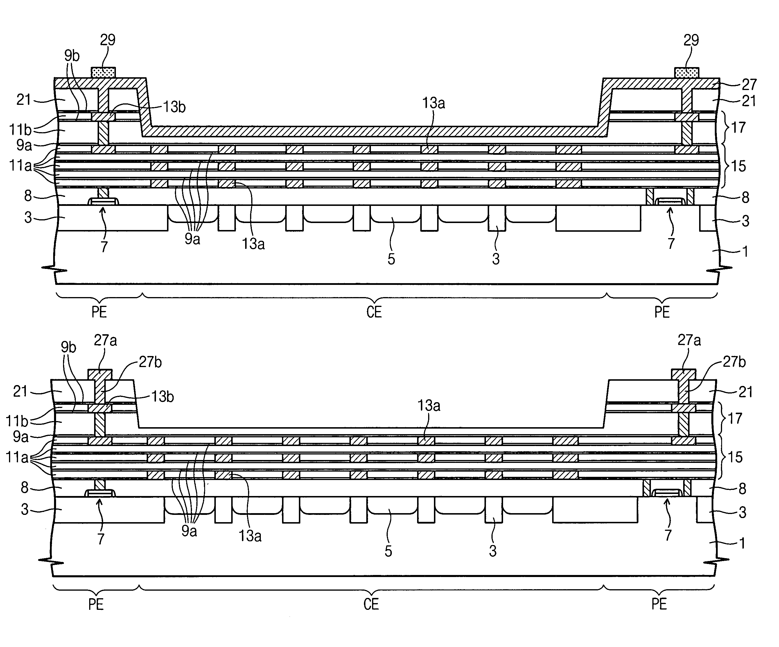
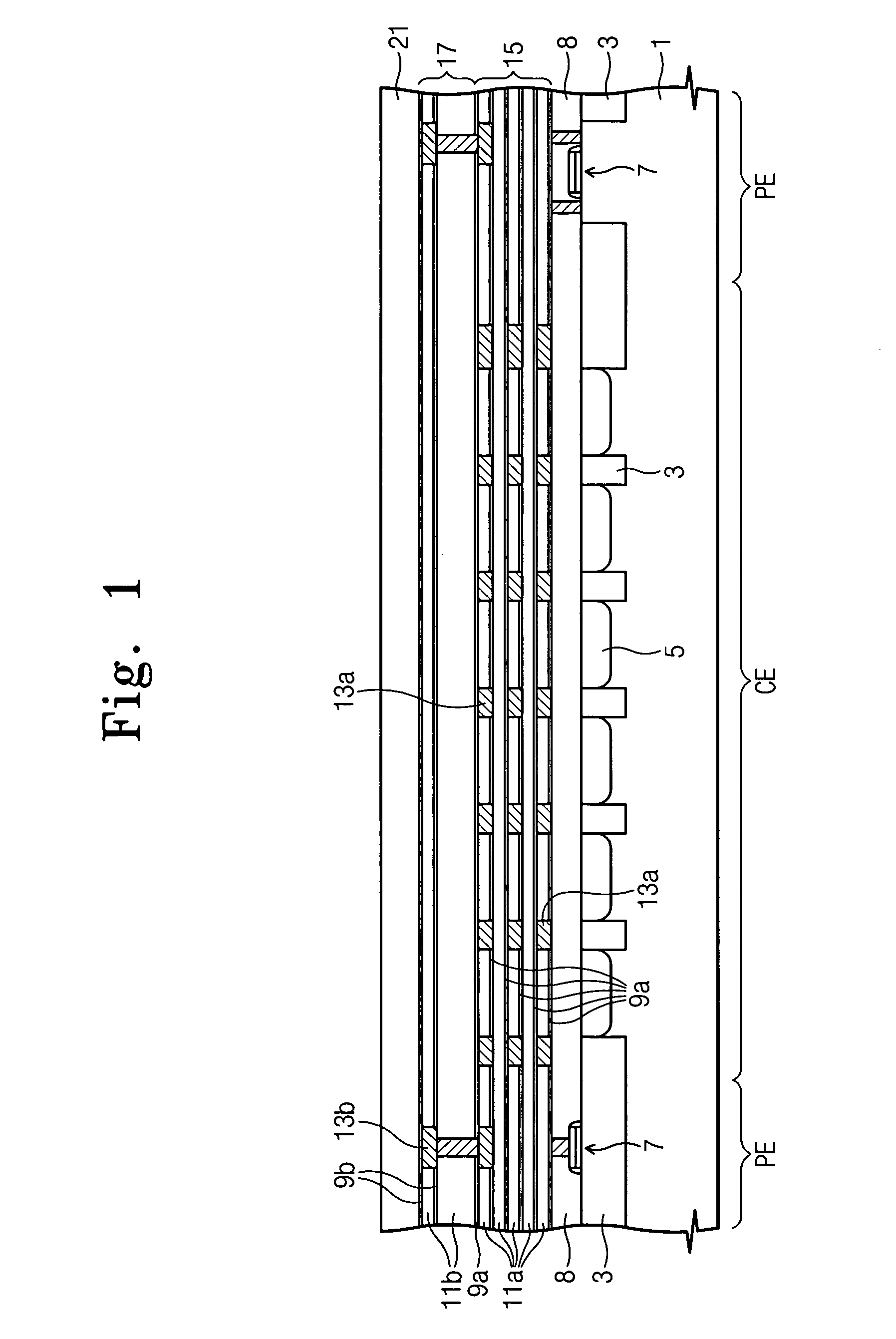
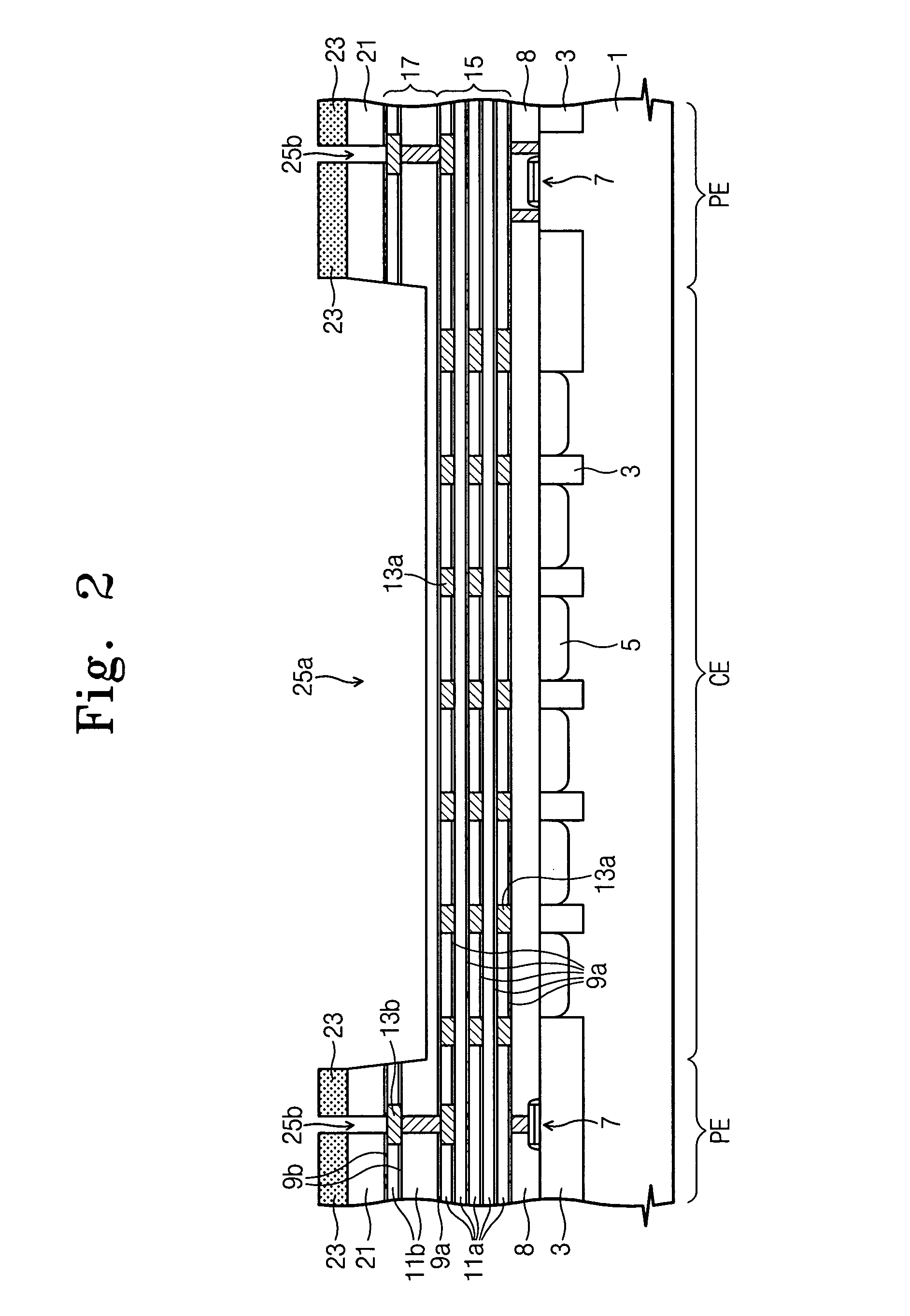
The present invention provides methods for forming image sensors with improved conductivity and reliability. The methods involve forming a photoelectric transformation section at the semiconductor substrate, adding interlayer dielectrics and interconnections, and etching to expose the interconnections. A conductive layer is then formed to fill the via hole and a passivation layer is partially patterned to form a via plug and conductive pad at the peripheral circuit region. The image sensor includes a semiconductor substrate with a pixel region and a peripheral circuit region, device isolation layers, a photoelectric transformation section, a shield layer, intermediate interconnection layers, a passivation layer, a via plug, and a conductive pad at the peripheral circuit region. The methods and image sensor provide improved performance and reliability for image sensors.

Problems solved by technology

CCD image sensors on the other hand exhibit high power consumption and are generally not suitable for high integration processes.

Method used


Image

  • Image sensor and method for forming the same
  • Image sensor and method for forming the same
  • Image sensor and method for forming the same

Examples


Embodiment Construction

[0012]The present invention will now be described more fully hereinafter with reference to the accompanying drawings, in which preferred embodiments of the invention are shown. The invention may, however, be embodied in different forms and should not be construed as limited to the embodiments set forth herein. The invention may be applied to, for example, methods of forming CMOS or CCD image sensors. In the drawings, the height of layers and regions are exaggerated for clarity. It will also be understood that when a layer is referred to as being “on” another layer or substrate, it can be directly on the other layer or substrate, or intervening layers may also be present. Like numbers refer to like elements throughout.

[0013]As illustrated in the exemplary embodiment of FIGS. 1-6, device isolation layers 3 are formed at a semiconductor substrate 1 having a pixel region CE and a peripheral circuit region PE to define active regions. Impurities are implanted into the active region to fo...


PUM


Abstract

A method for forming an image sensor is provided. The method includes providing a semiconductor substrate having a pixel region and a peripheral circuit region, forming a photoelectric transformation section at the semiconductor substrate of the pixel region, forming a plurality of interlayer dielectrics over the semiconductor substrate with interconnections interposed therebetween, forming a passivation layer, partially patterning the passivation layer at the peripheral circuit region to form a via hole exposing the interconnection and removing the passivation layer and the underlying interlayer dielectric at the pixel region. The method further includes forming a conductive layer to fill the via hole and etching the conductive layer to remove the conductive layer at the pixel region and form a via plug and a conductive pad at the peripheral circuit region. The via plug fills the via hole and the conductive pad protrudes outwardly from the via hole.

Description

PRIORITY STATEMENT[0001]This application claims priority of Korean Patent Application No. 2005-09541, filed on Feb. 2, 2005 in the Korean Intellectual Property Office, the disclosure of which is incorporated by reference herein in its entirety.BACKGROUND OF THE INVENTION[0002]1. Field of the Invention[0003]The present invention is directed to image sensors and to methods for forming the same.[0004]2. Description of Related Art[0005]Image sensors are semiconductor devices for converting an optical image into an electrical signal. Generally, image sensors are classified into charge coupled devices (CCDs) or complementary metal-oxide-silicon (CMOS) image sensors. CCD image sensors have certain benefits over CMOS image sensors such as having higher photosensitivity and better noise characteristics in comparison to CMOS image sensors. However, CMOS image sensors also hold several key benefits over CCD image sensors in that for example, CMOS image sensors may be prepared by simple process...

Claims


Application Information

Patent Timeline
Patent Type & Authority Patents(United States)
IPC IPC(8): H01L21/00
CPCH01L27/14627H01L27/14636B42D1/007B42F5/00B42F21/04B42P2221/04B42P2241/16G09B3/00
Inventor KIM, KI-HONG
Owner SAMSUNG ELECTRONICS CO LTD
Learn More