Method for manufacturing semiconductor devices

a manufacturing method and technology for semiconductor devices, applied in the direction of semiconductor devices, basic electric elements, electrical equipment, etc., can solve the problems of low selectivity of gas for polysilicon and siosub>2/sub>, and achieve the effect of improving the shape of the etched interlayer insulating layer and reducing the amount of deposits

Inactive Publication Date: 2008-04-29
HITACHI HIGH-TECH CORP
View PDF6 Cites 158 Cited by
  • Summary
  • Abstract
  • Description
  • Claims
  • Application Information

AI Technical Summary

Benefits of technology

[0020]Since the gas mixture is used to etch the interlayer insulating layer, a large amount of deposits are formed on walls of the etched interlayer insulating layer and the walls are likely to be tapered. However, the amount of the deposits can be reduced and the shape of the etched interlayer insulating layer can be improved without sacrificing the etching selectivity of Al2O3 to polysilicon or SiO2 in such a manner that the sample is maintained at high temperature.

Problems solved by technology

However, such gas has low selectivity for polysilicon and SiO2.
Therefore, if the gas is used, the following problem occurs: a problem that the first polysilicon layers 204 and the base insulating layers (gate oxide layers) 205 placed thereunder are etched during the removal of Al2O3 present around steps.

Method used


Image

  • Method for manufacturing semiconductor devices
  • Method for manufacturing semiconductor devices
  • Method for manufacturing semiconductor devices

Examples


Embodiment Construction

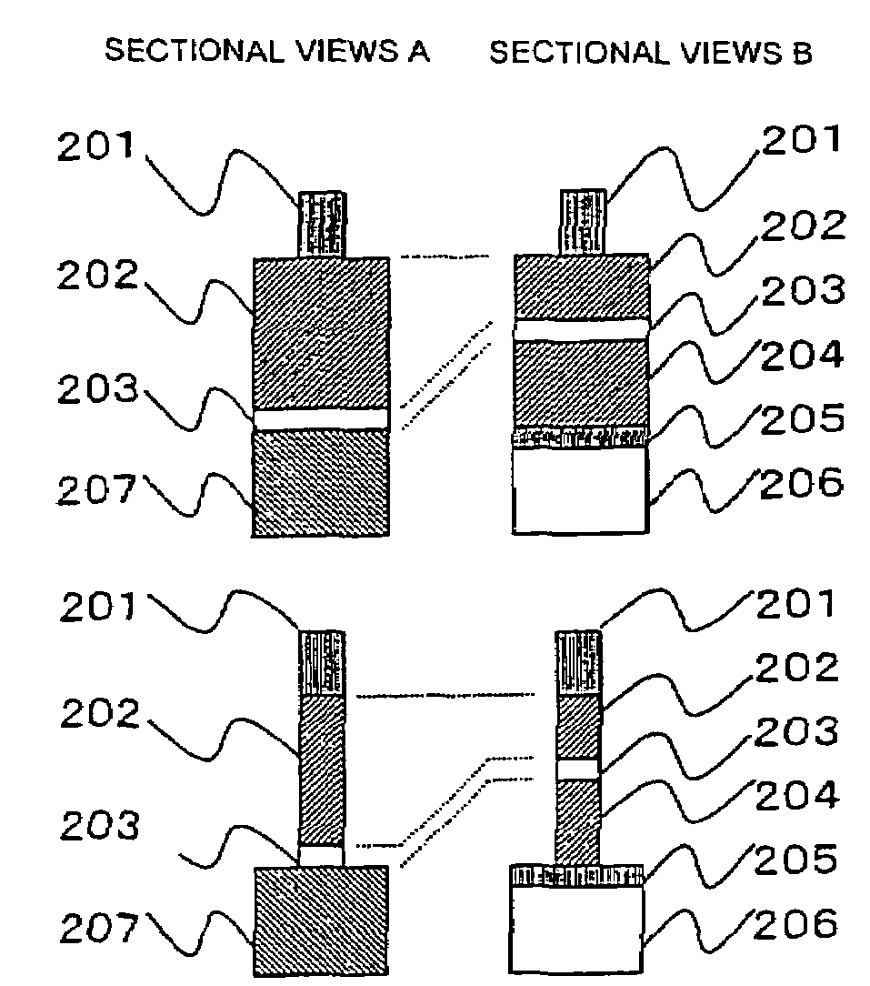
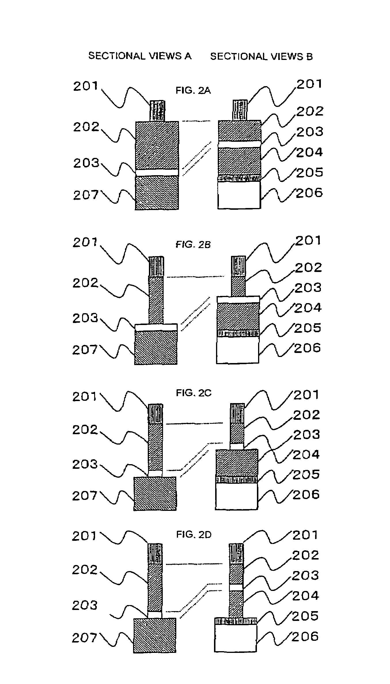
[0025]The present invention provides a method for manufacturing semiconductor devices by etching a sample including an Al2O3 interlayer insulating layer and polysilicon or SiO2 layers in contact with the Al2O3 interlayer insulating layer using a plasma etching system and a gas mixture containing BCl3, Ar, and CH4 or He.

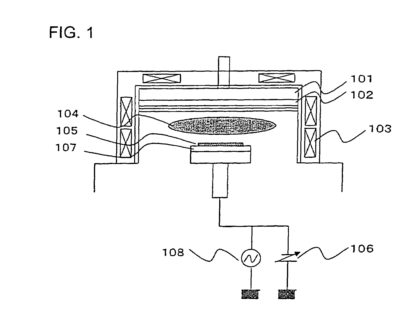
[0026]The method according to the present invention will now be described. A plasma-generating section included in the plasma etching system is described in detail with reference to FIG. 1. In order to generate plasma, UHF waves and a magnetic field are used. The UHF waves are transmitted from a UHF power supply and reach an etching chamber through an antenna 101 and then a UHF wave-transmitting plate 102. The resulting UHF waves induce electron cyclotron resonance (ECR) under the action of the magnetic field generated from a solenoid coil 103 surrounding the etching chamber, thereby generating high-density plasma from process gas in the etching chamber.

[0027]After th...


PUM


Abstract

A method for manufacturing semiconductor devices includes a step of etching a sample including an interlayer insulating layer containing Al2O3 and a polysilicon or SiO2 layer in contact with the interlayer insulating layer using a plasma etching system. The interlayer insulating layer is etched with a gas mixture containing BCl3, Ar, and CH4 or He. The gas mixture further contains Cl2. The interlayer insulating layer is etched in such a manner that a time-modulated high-frequency bias voltage is applied to the sample. The interlayer insulating layer is etched in such a manner that the sample is maintained at a temperature of 100° C. to 200° C. The interlayer insulating layer and the polysilicon or SiO2 layer are separately etched in different chambers.

Description

[0001]The present application is based on and claims priority of Japanese patent application No. 2005-216084 filed on Jul. 26, 2005, the entire contents of which are hereby incorporated by reference.BACKGROUND OF THE INVENTION[0002]1. Field of the Invention[0003]The present invention relates to a method for manufacturing semiconductor devices including alumina (Al2O3) layers and polysilicon or silicon dioxide (SiO2) layers placed thereunder. The method includes steps of selectively processing these layers.[0004]2. Description of the Related Art[0005]Al2O3 that is a high-K material is used to manufacture fine semiconductor devices. In particular, Al2O3 is used to form insulating layers placed between control gates and floating gates included in flash devices. The two types of gates are made of polysilicon and isolated from each other. In order to manufacture the flash devices, polysilicon layers for forming the control and floating gates and the Al2O3 insulating layers are selectivel...

Claims


Application Information

Patent Timeline
Patent Type & Authority Patents(United States)
IPC IPC(8): H01L21/336
CPCH01L21/28273H01L21/31122H01L21/823437H01L29/40114H01L21/306
Inventor SAITO, GONISHIDA, TOSHIAKISHIMOMURA, TAKAHIROARASE, TAKAO
Owner HITACHI HIGH-TECH CORP
Why Eureka
Try Eureka