

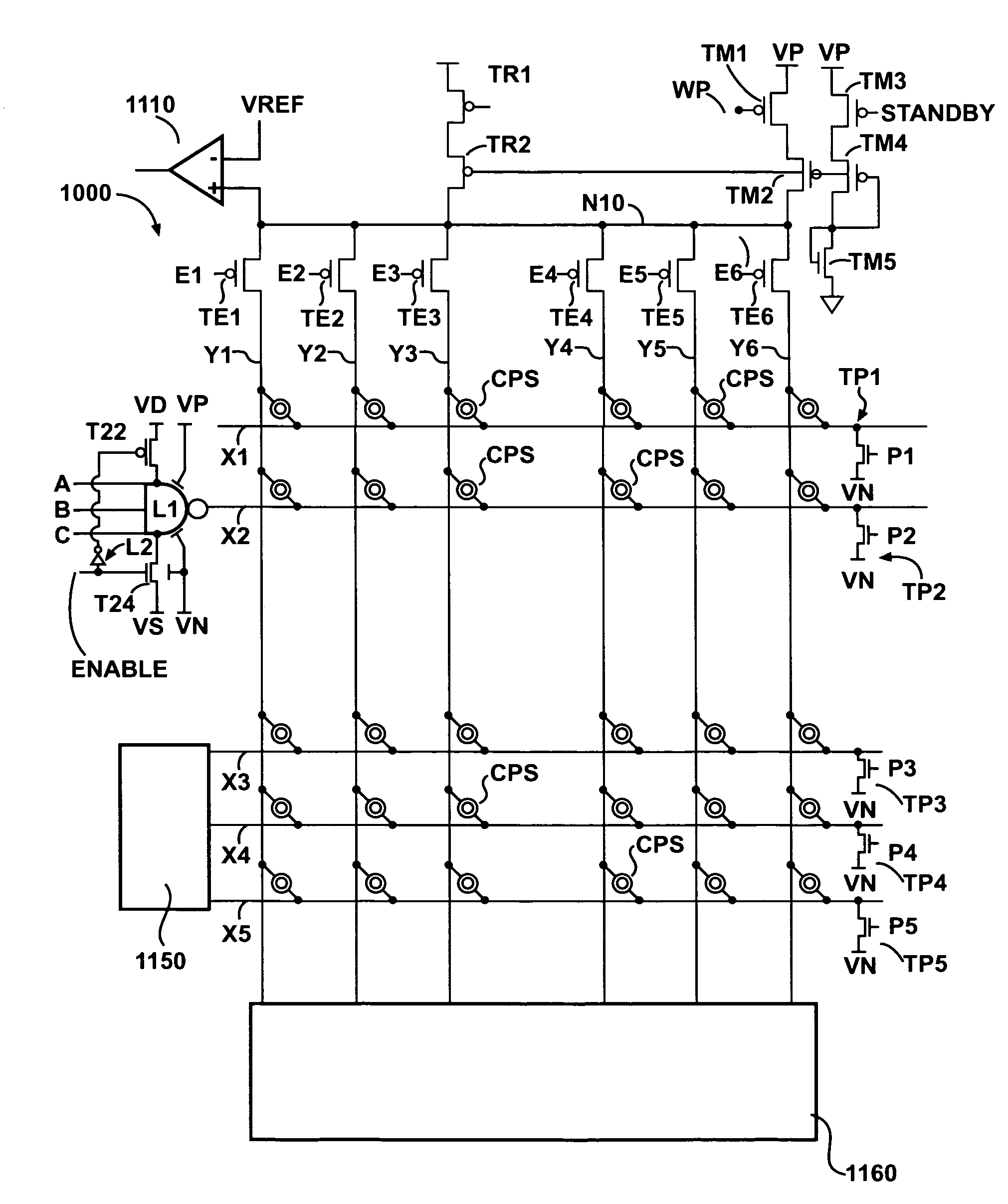
Programmable matrix array with phase-change material
a phase-change material and matrix array technology, applied in logic circuits using specific components, pulse techniques, instruments, etc., can solve the problems of delayed restart, power draining by the intended cross-points, and high tooling costs and time delay of first article products, so as to reduce programming overhead area, improve efficiency and cost, and facilitate and efficiently opera
- Summary
- Abstract
- Description
- Claims
- Application Information
AI Technical Summary
Benefits of technology
Problems solved by technology
Method used
Image

Examples
case 1
ogrammable connection comprises a phase-change material:
[0121]->it is labeled as CPS
Case 2: The programmable connection comprises a phase-change material but does not include a breakdown layer:[0122]->it is labeled as WCPS
Case 3: The programmable connection comprises a phase-change material and a breakdown layer:[0123]->it is labeled as BCPS
Case 3a: The programmable connection comprises a phase-change material and a breakdown layer. In addition, we wish to denote that the breakdown layer is broken down or popped to create a conductive pathway:[0124]->it is labeled as BCPS_B
Case 3b: The programmable connection comprises a phase-change material and a breakdown layer. In addition we wish to denote that the breakdown layer is not broken down but is instead intact:[0125]->it is labeled as BCPS_NB
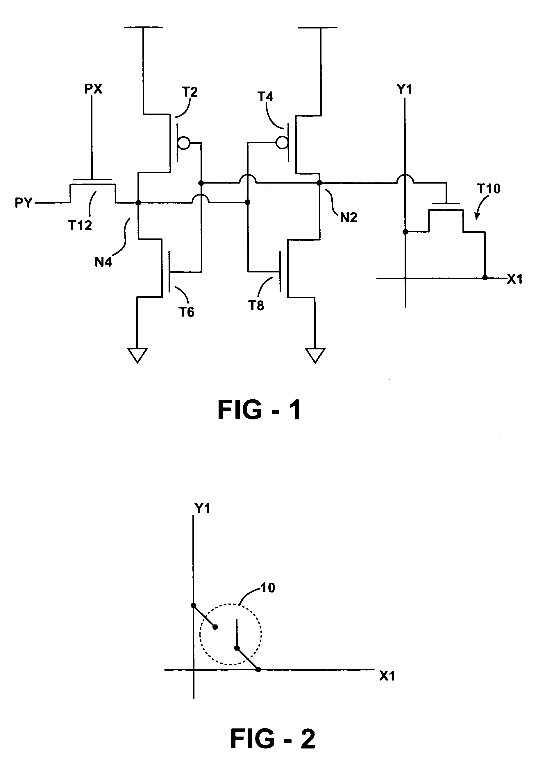
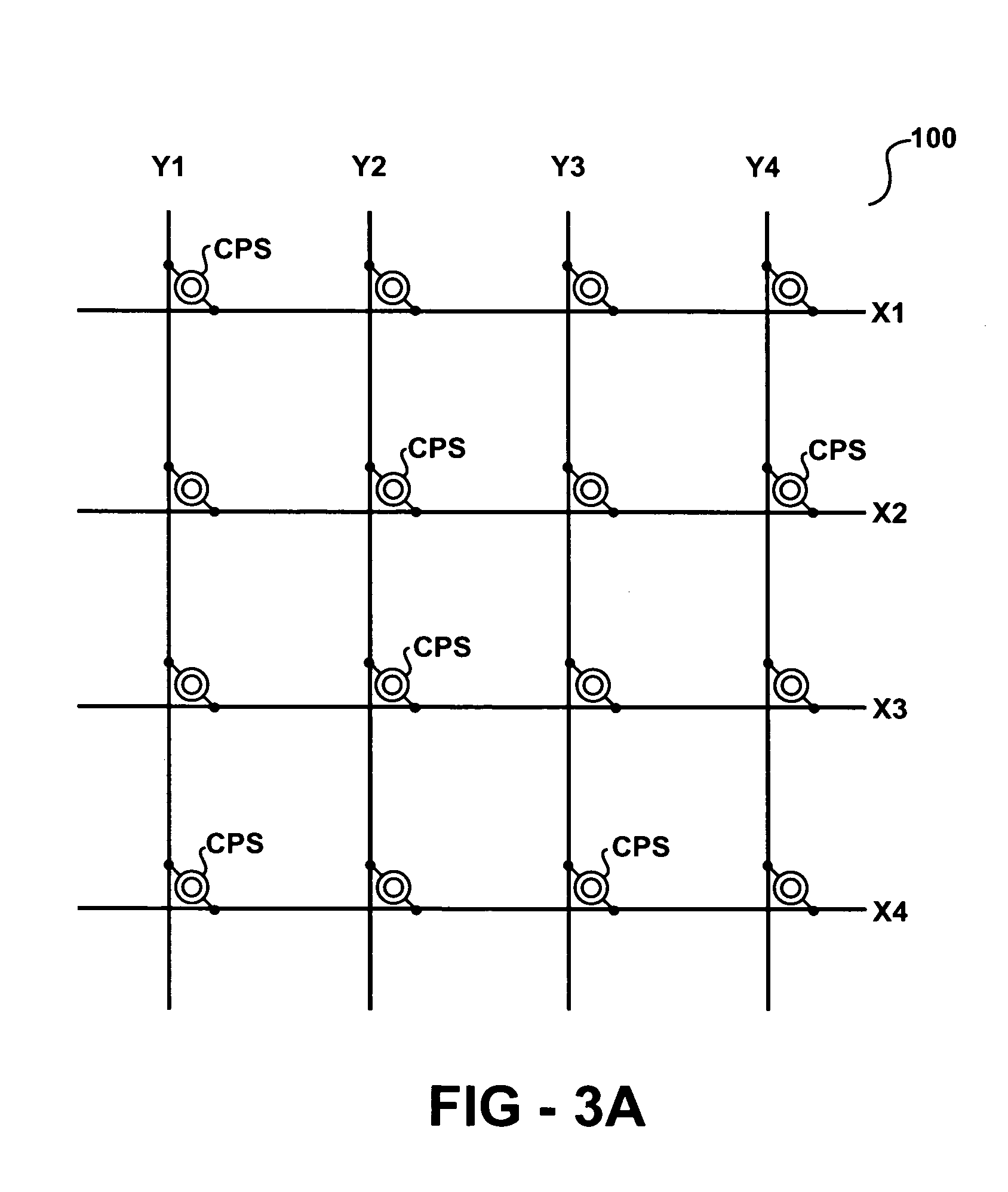
[0126]FIGS. 11a through 11D show symbols that represent each of programmable connection states CPS, WCPS, BCPS_NB and BCPS_B, respectively. In addition, FIG. 11E shows a symbol for a direct conne...
PUM
 Abstract
Description
Claims
Application Information