Fast response liquid crystal mode

a liquid crystal mode and fast response technology, applied in non-linear optics, instruments, optics, etc., can solve the problems of increasing fabrication difficulty, limited switching speed and limiting application of nematic liquid crystals today, and achieves high stability and fast relaxation

Active Publication Date: 2008-05-06
UNIV OF CENT FLORIDA RES FOUND INC
View PDF9 Cites 28 Cited by
  • Summary
  • Abstract
  • Description
  • Claims
  • Application Information

AI Technical Summary

Benefits of technology

[0014]The fourth objective of the present invention is to provide a fast-response liquid crystal modulator with self-imposed strong boundary layers such that very fast relaxation occurs even in a thick cell.
[0015]The fifth objective of the present invention is to provide a fast-response liquid crystal modulator with high stability.

Problems solved by technology

Due to the slow response of nematic liquid crystals (typically 25 milliseconds (ms) to 100 ms), applications for nematic liquid crystals today have been mainly limited to those with relatively low data rates.
This shortcoming is caused by the fact that the switching speed of nematic liquid crystals is often limited by its long relaxation time.
This thin cell gap however increases fabrication difficulty, especially when the panel size is large, and also limits the potential optical retardation since cell gap is limited.
Although a liquid crystal mode, known as Pi-cell Bend mode or Optically Compensated Bend (OCB) mode, capable of generating very fast response without the use of thin cell gap has been reported, this liquid crystal mode is unstable and requires a constant bias voltage.
The VA-IPS mode can achieve a wide-viewing angle property but the response time is not very fast.
Therefore the electric field in the VA-IPS mode is much more spread out and less localized which results in large switching of LC bulk layer and hence small boundary effect and slower response time.
The OCB mode is however rather unstable since it involves the Splay to Bend transition and it also requires a constant bias voltage.

Method used


Image

  • Fast response liquid crystal mode
  • Fast response liquid crystal mode
  • Fast response liquid crystal mode

Examples


Embodiment Construction

[0043]Before explaining the disclosed embodiment of the present invention in detail it is to be understood that the invention is not limited in its application to the details of the particular arrangement shown since the invention is capable of other embodiments. Also, the terminology used herein is for the purpose of description and not of limitation.

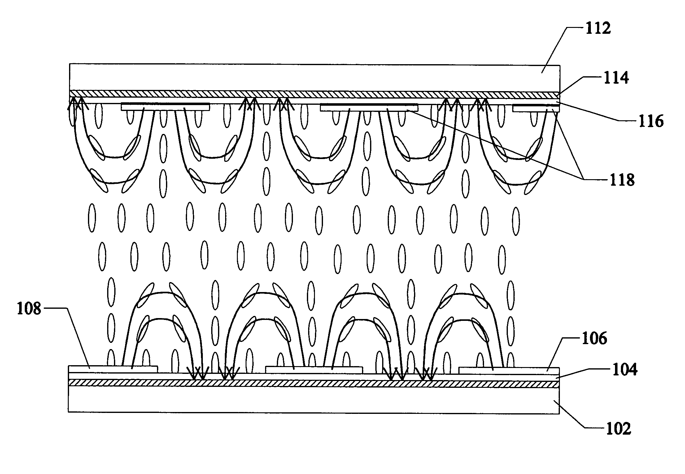
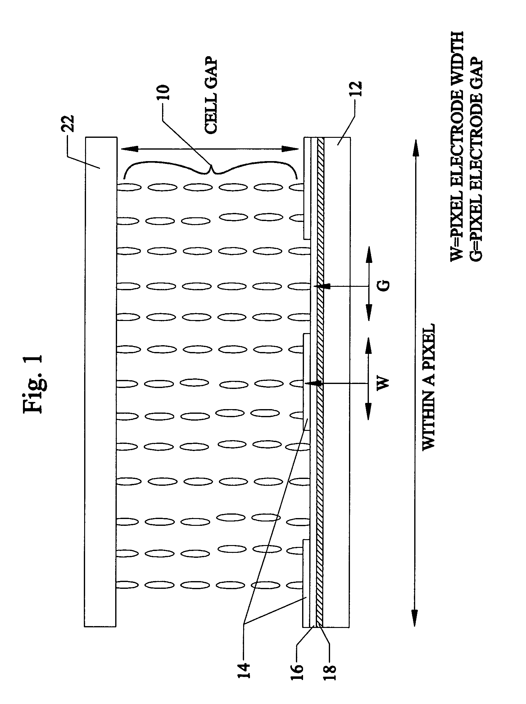
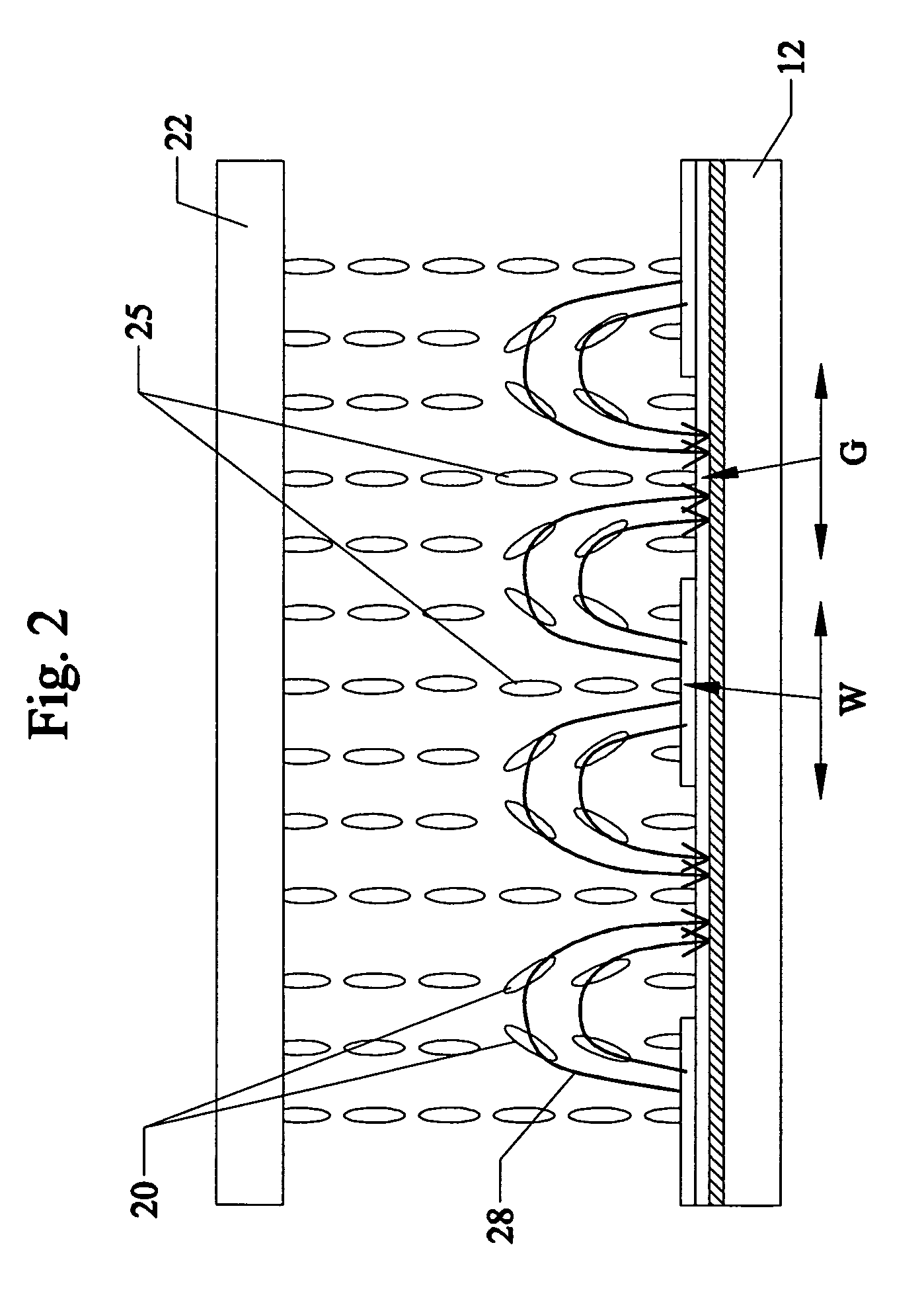
[0044]Acronyms used throughout the description of the present invention are defined as follows:[0045]G—pixel electrode gap measured in micrometers (μm)[0046]LC—liquid crystal[0047]OCB—Optically Compensated Bend liquid crystal mode requires continuous application of bias voltage.[0048]PA—Parallel Alignment of liquid crystals[0049]TN—Twisted Nematic liquid crystals[0050]VA-FFS—Vertical Alignment Fringing Field Switching liquid crystal mode of the present invention uses very low voltage, e.g., [0051]VA-IPS—Vertical Alignment In Plane Switching liquid crystal mode[0052]W—pixel electrode width measured in micrometers (μm)

[0053]The operating...


PUM

PropertyMeasurementUnit
widthaaaaaaaaaa
lengthaaaaaaaaaa
widthaaaaaaaaaa

Abstract

A novel nematic liquid crystal (LC) mode is based on the Fringing-Field-Switching of Vertically-Aligned liquid crystals. The VA-FFS mode is capable of generating very fast optical modulation without the use of very thin cell gap. IA major feature of this LC mode is that it has unusual fast relaxation time compared with the conventional nematic LC modes that require a thin cell gap. This fast relaxation occurs even at very low applied voltages and the operation is very stable. The fast-response mechanism of this LC mode involves the confinement of liquid crystal molecular switching within self-imposed thin LC layers. The present invention provides a novel approach to overcome the fundamental problem of the long relaxation time of the conventional nematic liquid crystal modes.

Description

[0001]This invention was supported in part by Department of Defense Advanced Research Project Agency (DARPA) and Raytheon Electronic Systems under Contract No. 65-04-878.[0002]This invention claims the priority of U.S. Provisional Application Ser. No. 60 / 480,622 filed Jun. 23, 2003.FIELD OF THE INVENTION[0003]This invention relates to a liquid crystal operation mode, and in particular to methods and apparatus for producing a stable and fast-response optical modulator for use in optical communications and advanced display systems.BACKGROUND AND PRIOR ART[0004]Due to the slow response of nematic liquid crystals (typically 25 milliseconds (ms) to 100 ms), applications for nematic liquid crystals today have been mainly limited to those with relatively low data rates. This shortcoming is caused by the fact that the switching speed of nematic liquid crystals is often limited by its long relaxation time. Unlike the switching-on process, which is electric-field driven, the relaxation proces...

Claims


Application Information

Patent Timeline
Patent Type & Authority Patents(United States)
IPC IPC(8): G02F1/1343G02F1/1337
CPCG02F1/134363G02F1/1393G02F2001/134372G02F1/134372
Inventor CHOI, WING KITWU, SHIN-TSON
Owner UNIV OF CENT FLORIDA RES FOUND INC
Why Eureka
Try Eureka