Fast calibration of electronic components

a technology of electronic components and fast calibration, applied in the direction of instruments, transmission monitoring, baseband system details, etc., can solve the problems of unwanted signal interference, information loss, signal fidelity degradation,

Inactive Publication Date: 2008-05-06
FINGERPRINT CARDS AB
View PDF10 Cites 14 Cited by
  • Summary
  • Abstract
  • Description
  • Claims
  • Application Information

AI Technical Summary

Benefits of technology

[0015]Accordingly, the present invention is directed to a fast calibration method that substantially obviates one or more of the shortcomings or problems due to the limitations and disadvantages of the related art.

Problems solved by technology

However, several factors can contribute degradation of the signal fidelity from the time the signal is created, transmitted, received and reproduced.
As a signal is processed using analog and / or digital processing (DSP) techniques, gain, offset and imbalances of phase may cause errors to be introduced into the signal, which can result in the loss of information and cause unwanted signal interferers.
Baseband signals are not usually suitable for direct transmission over the communications medium because of their relatively low frequency.
Self-mixing is mainly a concern in demodulation because LO-leakage at the demodulator input causes undesirable DC offset to appear at the demodulator output, for example, when down-converting a bandpass signal to baseband.
On the other hand, LO-leakage at a modulator output often is the result of having DC offset present at the modulator input.
In an RF mixer, there will always be some amount of leakage of the LO signal.
In some applications, there is a need to provide DC compensation to minimize LO-leakage because LO-leakage impairs the modulation accuracy.
However, the number of combinations in a two-dimensional configuration leads to delays during the production of circuit components because it is often necessary to make an excessive number of measurements before determining a setting for an acceptable LO-leakage level, or before a determination can be made as to whether it is necessary to discard the circuit component entirely (e.g., when LO-leakage is greater than can be compensated for by any combination of the bits associated with each of the I and Q channels).
The conventional methods for setting DC offset compensation are cumbersome, time consuming and cause excessive wear on production facilities, resulting in reduced output production and increased costs.
In some instances, sign shifts may increase a level of complexity to a calibration process, but most often do not present serious problems.

Method used


Image

  • Fast calibration of electronic components
  • Fast calibration of electronic components
  • Fast calibration of electronic components

Examples


Embodiment Construction

[0035]These and other aspects of the invention will now be described in greater detail in connection with exemplary embodiments that are illustrated in the accompanying drawings.

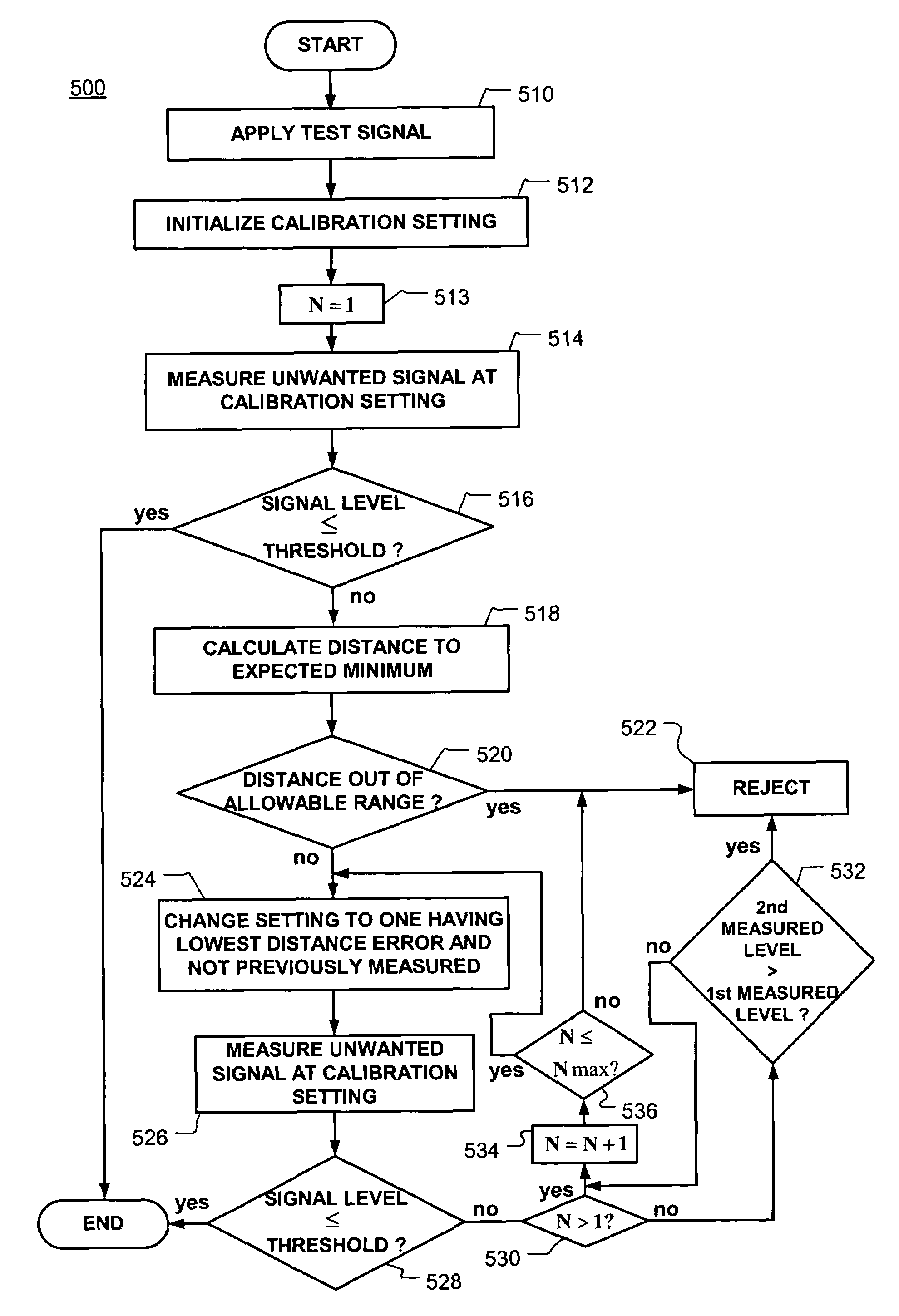
[0036]One problem with conventional methods of calibration is that the number of measurements needed to find a required DC-offset compensation setting often exceeds an acceptable number of attempted measurements. One conventional method also involves making at least 9 measurements for a 7×7 grid before it can be determined that a device cannot be calibrated within a range of possible DC compensation settings. However, as the size of the grid is increased, so too is the number of possible settings. Hence, when using the above conventional method an increase in grid size would require a corresponding increase in the number of measurements needed before a determination can be made that a device cannot be calibrated. Even in the case of calibrating in only one dimension, the above conventional method for a 7×7 g...


PUM


Abstract

The number of measurements needed to calibrate an electrical device is reduced. Apparatus and methods minimize output of one or more unwanted signals by determining a calibration setting, in a minimal number of measurements, from determined distances to a best setting. Each distance to a best setting can be determined as a function of the characteristic of the unwanted signal and the measured unwanted signal level. A calibration setting point can be determined by searching for a setting point having a lowest sum of distance errors determined from the calculated distances and from the measured and non measured setting points. The techniques and apparatus are useful for minimizing a number of measurements that would be needed for determining a setting that substantially prevents generation of unwanted output signals, such as carrier leakage (LO-leakage) and unwanted sidebands, and for quickly determining whether an acceptable calibration setting exists for a device.

Description

RELATED APPLICATION[0001]This application is related to, and claims priority from U.S. Provisional Application Ser. No. 60 / 470,221 entitled “Fast Calibration of DC-Offset Compensation” filed on May 14, 2003, the entire disclosure of which is expressly incorporated herein by reference.BACKGROUND OF THE INVENTION[0002]1. Field of the Invention[0003]The present invention relates to calibration of electronic devices, and more particularly, to techniques for efficiently calibrating these devices to prevent or reduce unwanted signals at the device output.[0004]2. Description of the Related Art[0005]It is often required that the input-output relationship of electronic components be predictable and accurate. For instance, in communication systems, signals conveying information that are transmitted and received, such as voice or data, undergo processing in several stages both before transmission and upon reception. However, several factors can contribute degradation of the signal fidelity fr...

Claims


Application Information

Patent Timeline
Patent Type & Authority Patents(United States)
IPC IPC(8): H04B17/00H03C3/40H03D3/00H04L27/00
CPCH03C3/40H03D3/008H03D3/009H04L2027/0016
Inventor ANDERSSON, PETER
Owner FINGERPRINT CARDS AB
Why Eureka
Try Eureka