

Surface preparation for selective silicon fusion bonding
a surface preparation and selective silicon technology, applied in the field of fusion bonding methods, can solve the problems of limiting silicon fusion bonding, too large surface roughness to permit effective bonding, and reducing surface roughness
- Summary
- Abstract
- Description
- Claims
- Application Information
AI Technical Summary
Benefits of technology
Problems solved by technology
Method used
Image

Examples
Embodiment Construction
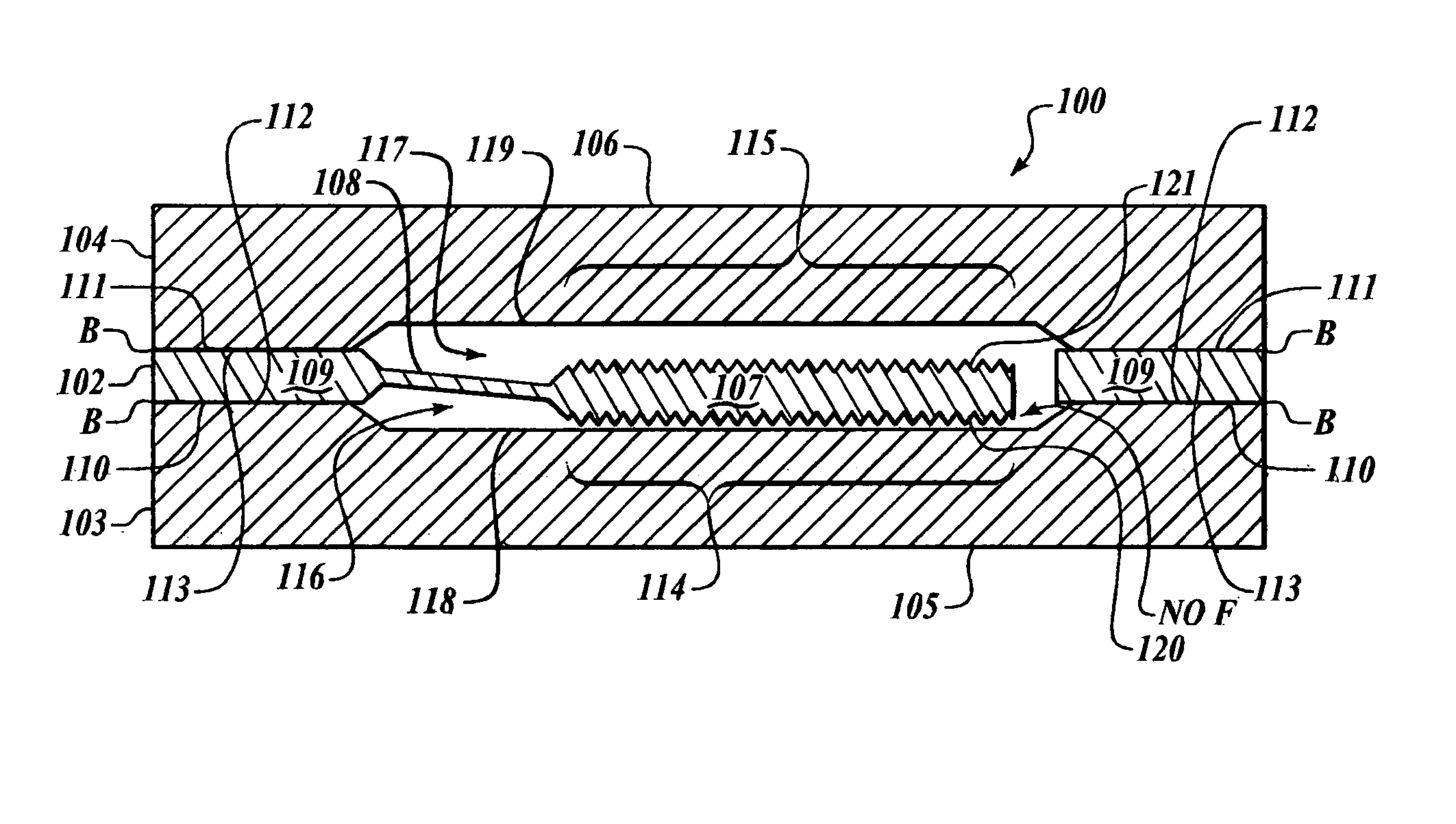
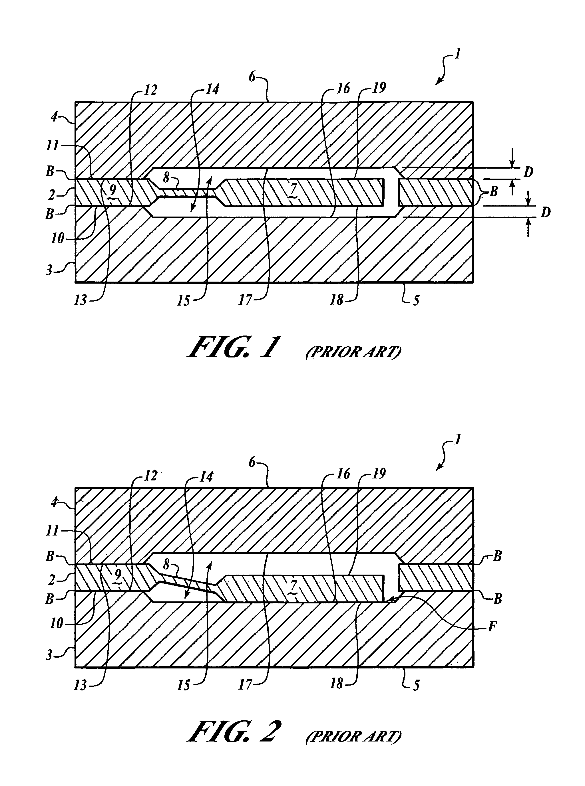
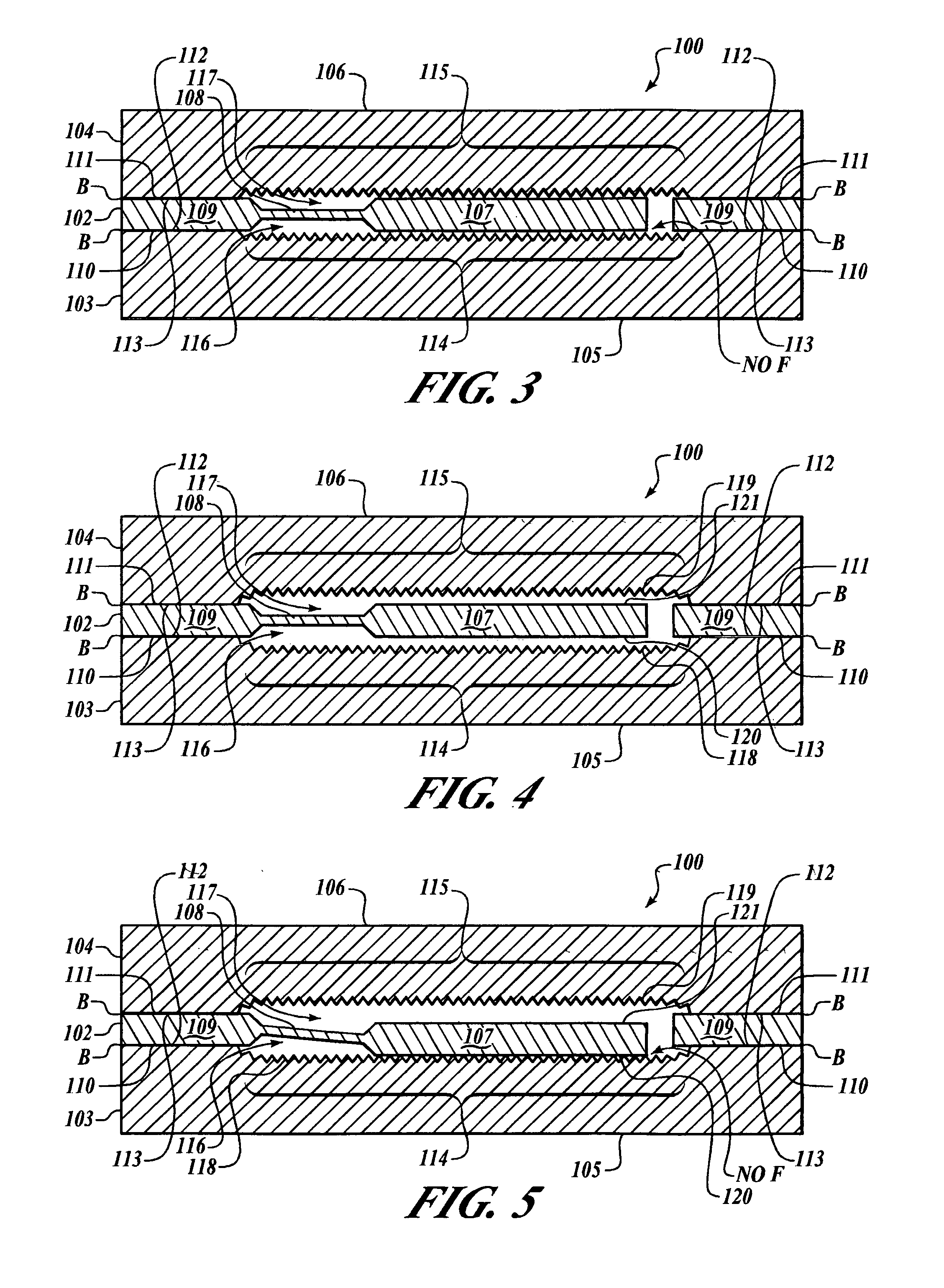
[0037]In the Figures, like numerals indicate like elements.
[0038]The Figures illustrate the method of the present invention for a monolithic silicon-based Micro-Electro Mechanical System (MEMS) device, such as a sensor or actuator, having opposing cover structures having respective substantially smooth and planar contact surfaces that are silicon fusion bonded to substantially smooth and planar opposing surfaces of a frame portion of a silicon mechanism structure, the mechanism structure being formed with one or more parts that are movable relative to the frame portion of the mechanism structure, wherein a relatively rough surface is disposed between the contact surface of one or both of the cover structures and a corresponding surface of the movable part of the mechanism structure.
[0039]According to one embodiment of the present invention, the relatively rough surface is disposed on the contact surface of one or both of the cover structures in an area thereof corresponding to the m...
PUM
 Abstract
Description
Claims
Application Information