Circuit board and manufacturing method thereof

a manufacturing method and circuit board technology, applied in the field of circuit boards, can solve the problems of inability to meet the trend of miniaturization of electrical products, the inability to effectively reduce the area of the circuit board, so as to reduce the time for manufacturing the circuit board and the manufacturing cost, the effect of narrow line width

Inactive Publication Date: 2008-06-03
GIGNO TECH CO LTD
View PDF14 Cites 12 Cited by
  • Summary
  • Abstract
  • Description
  • Claims
  • Application Information

AI Technical Summary

Benefits of technology

[0009]In view of the foregoing, the invention provides a circuit board and a manufacturing method thereof capable of effectively reducing the line width of the trace line or the pad size of the circuit board, shortening the time for manufacturing the circuit board, and reducing the manufacturing cost.
[0013]In brief, the circuit board of the invention and the method of manufacturing the same have the following advantages. Because the protrusion is formed by way of jetting and the first and second circuit layers may also be formed by way of jetting, no complicated procedures, such as the conventional printing or etching procedures, have to be performed. Thus, the circuit board and its manufacturing method of the invention can enable the reduction of the time for manufacturing the circuit board and the manufacturing cost. In addition, because the current jetting technology can achieve narrow line width down to 20 microns or smaller, the circuit board and its manufacturing method of the invention can effectively reduce the line width of the trace line or the pad size on the circuit board.

Problems solved by technology

However, owing to the limitation of the technology of forming the trace lines and the substrate material of the circuit board, the line width of the trace lines on the conventional circuit board or the size of the pads on the trace lines cannot be effectively reduced.
In other words, the area of the circuit board cannot be effectively reduced, making it impossible to meet the trend to miniaturize electrical products.
In addition, the trace lines and protrusions on the conventional circuit board have to be formed through complicated processes, so the manufacturing time or cost cannot be effectively shortened or reduced.

Method used


Image

  • Circuit board and manufacturing method thereof
  • Circuit board and manufacturing method thereof
  • Circuit board and manufacturing method thereof

Examples


Embodiment Construction

[0022]The present invention will be apparent from the following detailed description, which proceeds with reference to the accompanying drawings, wherein the same references relate to the same elements. It is to be noted that the circuit board of this invention may be the circuit board for carrying various active devices or passive devices, or the circuit board for carrying a chip or chips during the packaging process.

[0023]To make the invention more comprehensive, an example will be described hereinafter for illustrating a circuit board according to a preferred embodiment of the invention.

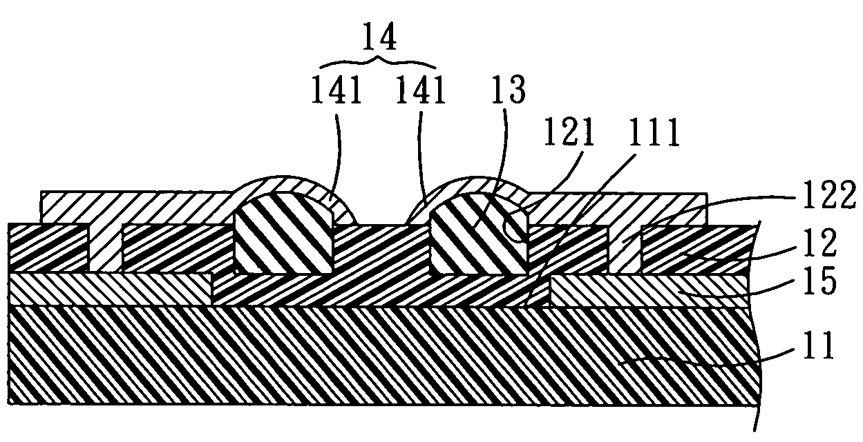
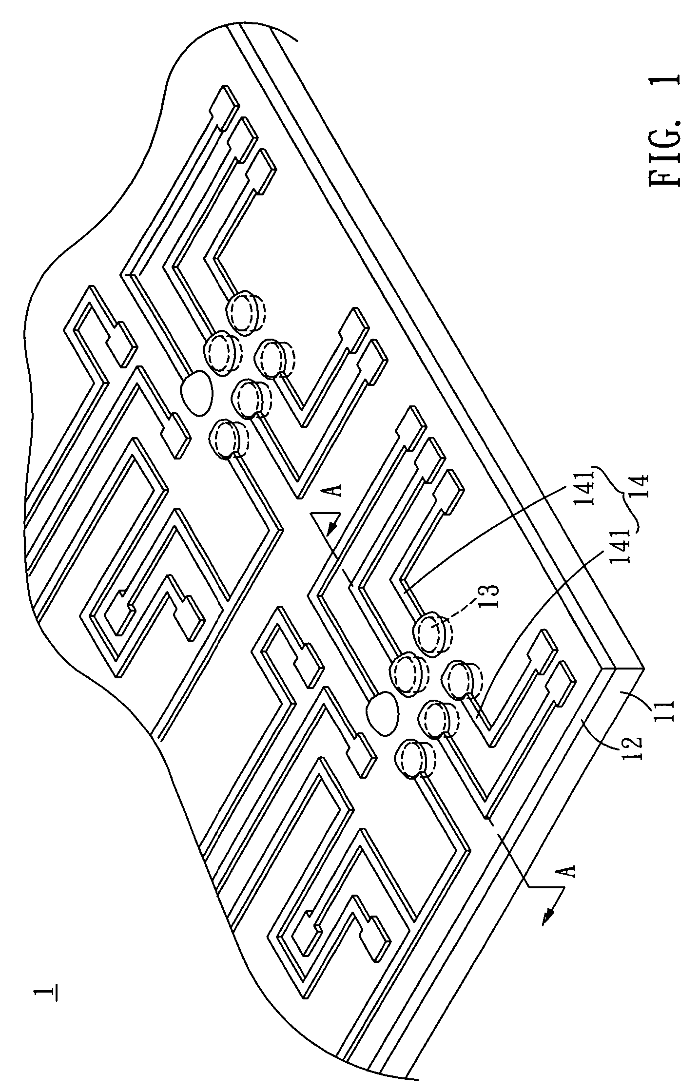
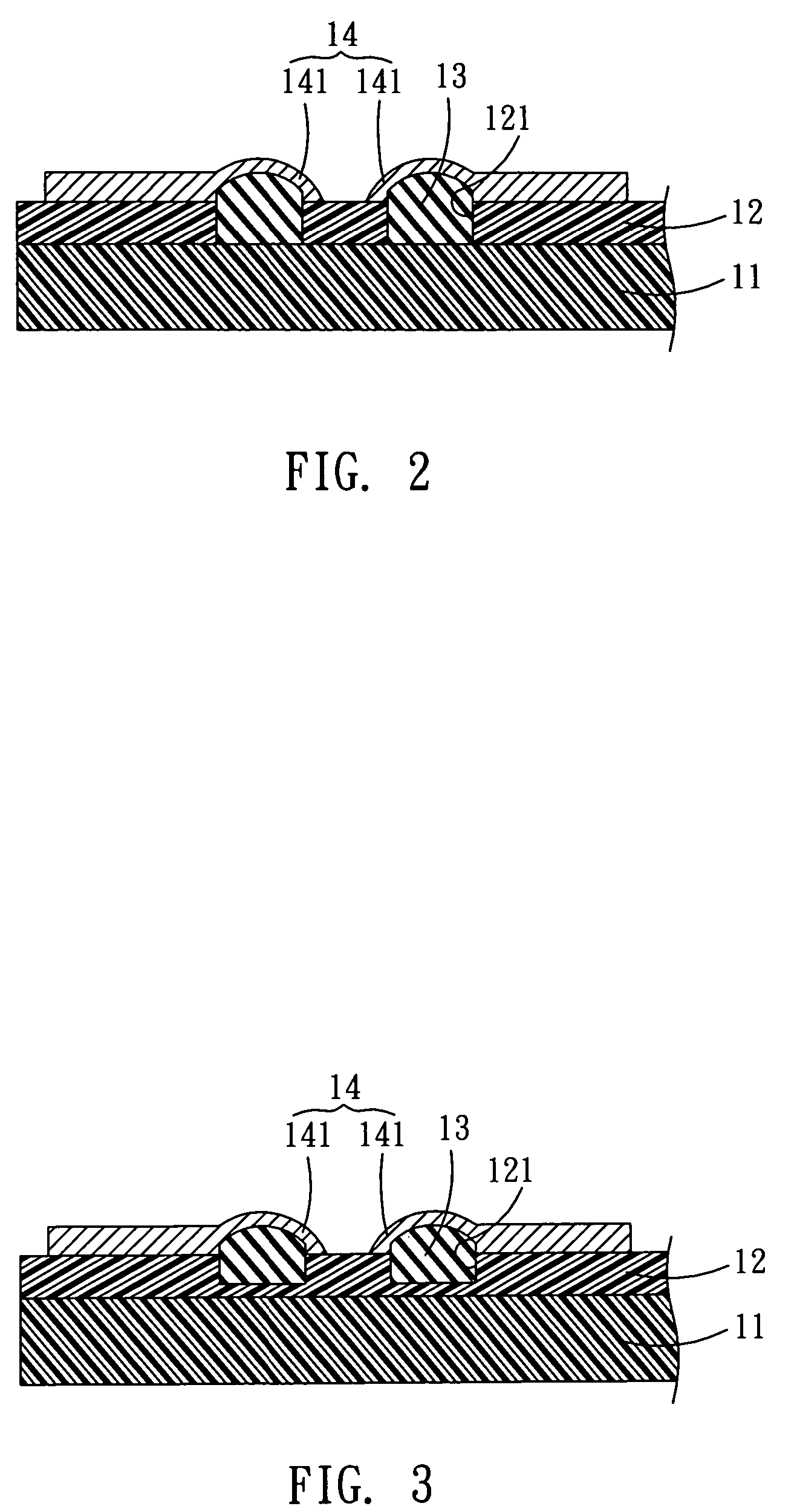
[0024]Referring to FIG. 1, the circuit board 1 of the invention includes a substrate 11, an insulating layer 12, at least one protrusion 13 and a first circuit layer 14.

[0025]As shown in FIG. 2, the insulating layer 12 is disposed on the substrate 11. The insulating layer 12 has at least one protrusion-positioning region 121. In this embodiment, the protrusion-positioning region 121 in the insulat...


PUM

PropertyMeasurementUnit
widthaaaaaaaaaa
sizeaaaaaaaaaa
electricalaaaaaaaaaa

Abstract

A circuit board includes a substrate, an insulating layer, at least one protrusion, and a first circuit layer. The insulating layer is disposed on the substrate and has at least one protrusion-positioning region. At least a part of the protrusion is disposed on the protrusion-positioning region. The first circuit layer is disposed on the insulating layer and has at least one trace line extending onto the protrusion.

Description

BACKGROUND OF THE INVENTION[0001]1. Field of Invention[0002]The invention relates to a circuit board and a method of manufacturing the same and more particularly to a circuit board formed by way of jetting and a method of manufacturing the same.[0003]2. Related Art[0004]Among the current electrical products, circuit boards, which are indispensable components, may be classified into many types. In terms of application, the circuit boards may be classified into printed circuit boards for carrying various active devices or passive devices, and carrier circuit boards for carrying chips during the packaging process.[0005]The printed circuit board is used for carrying various active devices or passive devices, on a trace line of which a pad is usually formed, or a protrusion may be formed on the pad in order to facilitate the electrical connection to the active device or passive device. In general, most of the protrusions formed on the printed circuit boards are solder bumps, gold protrus...

Claims


Application Information

Patent Timeline
Patent Type & Authority Patents(United States)
IPC IPC(8): H05K3/02H01R3/00H01R9/00H05K3/12
CPCH05K3/4007H05K1/0306H05K3/386H05K3/4644H05K2201/0133Y10T29/49155H05K2201/0367H05K2201/09909Y10T29/49149Y10T29/49158H05K2201/0187
Inventor LEE, YU-TUAN
Owner GIGNO TECH CO LTD
Why Eureka
Try Eureka