Capacitive/resistive devices, organic dielectric laminates and printed wiring boards incorporating such devices, and methods of making thereof

a technology of resistors and capacitors, applied in the direction of printed circuit non-printed electrical components association, conductive pattern formation, electrical apparatus construction details, etc., can solve the problems of increasing fabrication costs and reliability reduction of solder joints, so as to reduce the cost and difficulty of creating resistors and capacitor functions, free up valuable real estate, and improve reliability

Active Publication Date: 2008-06-03
CHEMTRON RES
View PDF32 Cites 18 Cited by
  • Summary
  • Abstract
  • Description
  • Claims
  • Application Information

AI Technical Summary

Benefits of technology

[0006]According to the above embodiment, both the resistor and the capacitor functions may be integrated into a single buried laminate, reducing the cost and difficulty in creating the resistor and capacitor functions. When the capacitive / resistive device is incorporated in a printed wiring board, embedding the capacitive / resistive device also frees up valuable real estate. Further, solder joints associated with SMT devices may be eliminated, thereby improving reliability. The capacitive / resistive device can be processed using conventional etching processes, further reducing production costs.

Problems solved by technology

Further, the requirement for solder joints reduces reliability and increases costs of fabrication.

Method used


Image

  • Capacitive/resistive devices, organic dielectric laminates and printed wiring boards incorporating such devices, and methods of making thereof
  • Capacitive/resistive devices, organic dielectric laminates and printed wiring boards incorporating such devices, and methods of making thereof
  • Capacitive/resistive devices, organic dielectric laminates and printed wiring boards incorporating such devices, and methods of making thereof

Examples


example 1

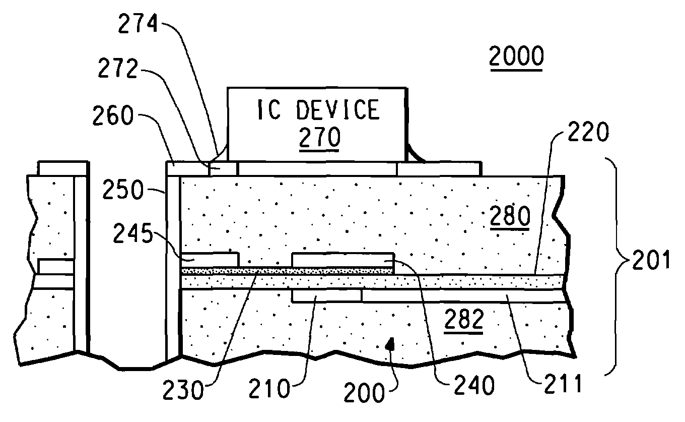
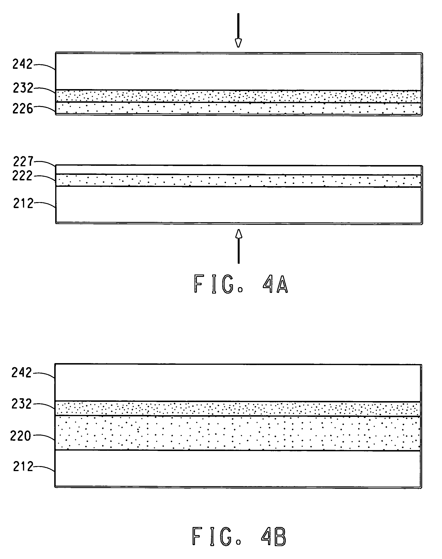
[0024]This example of the device 200 is discussed with reference to FIG. 3. In this example, the initial laminate structure shown in FIG. 4B, consists of copper foil 242 plated with a resistive material 232 that is composed of a nickel phosphorus alloy of sheet resistivity 50 ohms per square. The dielectric 220 is a barium titanate-filled thermoplastic polyimide. Barium titanate is advantageous as a filler as it is readily available and lead-free. The dielectric 220 is 14 microns thick and has a dielectric constant of 11, thereby yielding a capacitance density of 4.5 nanoFarads per square inch.

[0025]The size (when viewed from a top plan perspective) of the capacitor needed for a transmission line termination of 30 picoFarad is 4.3 square mm, or approximately 2 mm by 2 mm. Electrodes 210 and 240 are formed from etching copper foils 212 and 242. The above capacitor is easy to make to relatively high tolerances.

[0026]The size of the resistor in this example for a nominal 60 ohm resista...

example 2

[0027]This example of the device 200 is discussed with reference to FIG. 3. In this example, the initial laminate structure shown in FIG. 4B, consists of copper foil 242 plated with a resistive material 232 that is composed of a nickel phosphorus alloy of sheet resistivity 50 ohms per square. The dielectric 220 is a barium titanate-filled thermoplastic polyimide. Barium titanate is advantageous as a filler as it is readily available and lead-free. The dielectric 220 is 8 microns thick and has a dielectric constant of 11, thereby yielding a capacitance density of 6.2 nanoFarads per square inch.

[0028]The size (when viewed from a top plan perspective) of the capacitor needed for a transmission line termination of 30 picoFarad is 3.1 square mm, or approximately 1.77 mm by 1.77 mm. Electrodes 210 and 240 are formed from etching copper foils 212 and 242. The above capacitor is easy to make to relatively high tolerances.

[0029]The size of the resistor in this example for a nominal 60 ohm re...


PUM

PropertyMeasurementUnit
thicknessaaaaaaaaaa
dielectric constantaaaaaaaaaa

Abstract

A capacitive / resistive device provides both resistive and capacitive functions. The capacitive / resistive device may be embedded within a layer of a printed wiring board. Embedding the capacitive / resistive device conserves board surface real estate, and reduces the number of solder connections, thereby increasing reliability. Conserves board surface real estate, and reduces the number of solder connections, thereby increasing reliability.

Description

TECHNICAL FIELD[0001]The technical field relates to devices having both a capacitive and resistive functions, and methods of incorporating such devices in organic dielectric laminates and printed wiring boards.RELATED ART[0002]Capacitors and resistors may be used in series for transmission line termination of signal traces extending between integrated circuit (IC) devices. The capacitors and resistors are used to match the impedance of an IC device to a line, or to reduce or eliminate signal reflection. Some circuits are continuous load and use a resistor in parallel with the line. Non-continuous load circuits have a resistor and capacitor in series and are useful for low power ICs. FIG. 1 schematically illustrates a non-continuous load termination of IC devices 10 and 20 known in the prior art.[0003]In FIG. 1, the distance from a to b is typically short. The value of the resistor R is chosen to match the line impedance and is typically about 45-80 ohms. The value of the capacitor C...

Claims


Application Information

Patent Timeline
Patent Type & Authority Patents(United States)
IPC IPC(8): H05K1/18
CPCH01C7/005H01C17/06533H01C17/06586H01G4/40H05K1/162Y10T29/49155H05K3/429H05K2201/0209H05K2201/09309H05K2201/09763H05K1/167H05K1/16
Inventor BORLAND, WILLIAM J.COX, G. SIDNEYMCGREGOR, DAVID ROSS
Owner CHEMTRON RES
Why Eureka
Try Eureka