
Micro- and nano- hot embossing method for optical glass lens arrays

a technology of optical glass and hot embossing, which is applied in the field of glass molding, can solve the problems of reducing the service life of the mold and increasing the cost of mold manufacturing, and achieve the effects of improving the surface quality of the optical glass lens array, reducing cost, and large loss

Active Publication Date: 2020-10-22
NO 59 RES INST OF CHINA ORDNANCE IND +2
View PDF21 Cites 1 Cited by
  • Summary
  • Abstract
  • Description
  • Claims
  • Application Information

AI Technical Summary

Benefits of technology

The present invention provides a method for improving the surface quality of optical glass lens arrays and reducing the cost and difficulty of manufacturing them. This is achieved through a micro- and nano-hot embossing method that uses no expensive mold cores and reduces manufacturing difficulty. The method also improves the service life of the mold and reduces adhesion, friction, and shear between the glass element and the mold, resulting in improved surface quality of the optical glass lens array.

Problems solved by technology

However, when the micro-array optical glass elements are manufactured by micro- and nano-hot embossing, the surface quality and optical properties of the optical glass element are seriously influenced due to the coupling damage of fraction at high temperature and adhesion corrosion, thus greatly reducing the service life of the mold and then increasing the cost for manufacturing the mold.

Method used


Image

  • Micro- and nano- hot embossing method for optical glass lens arrays
  • Micro- and nano- hot embossing method for optical glass lens arrays

Examples


Embodiment Construction

eference to the embodiments, but these embodiments are not intended to limit the scope of the present invention. Simple substitutions and adjustments made by those skilled in the art according to the present invention shall fall within the scope of the present invention.

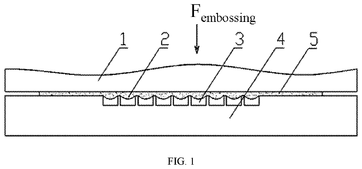
[0021]Taking L-BAL35 glass lens arrays as an example, a micro- and nano-hot embossing method for an optical glass lens array comprises the following steps.

[0022]1) A mold with a micro-hole array is prepared by micro EDM, where the size and contour of the micro-hole array match that of an optical glass lens array and the mold is made of a hard metal material which is conductive and meets strength and temperature requirements, and specifically, the mold is made of carbology, chrome-molybdenum steel or high-speed steel, and in this embodiment, the mold is made of carbology. During the processing of the micro-hole array using EDM, the pulse voltage is 120 V, the pulse frequency is 0.2 MHz, the pulse width is 500 ns, and ...


PUM

PropertyMeasurementUnit
Timeaaaaaaaaaa
Forceaaaaaaaaaa
Pressureaaaaaaaaaa

Abstract

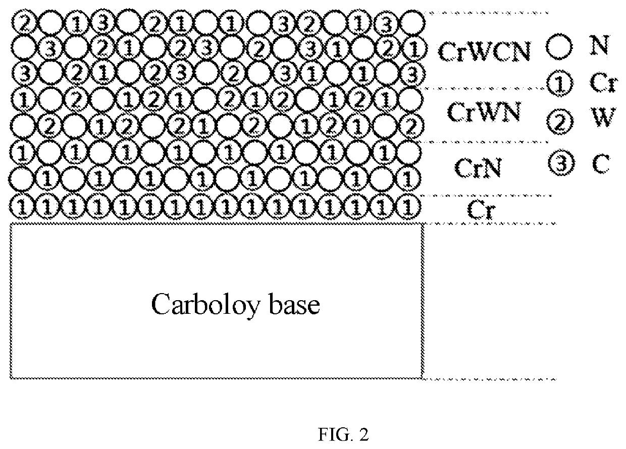
A micro- and nano-hot embossing method for an optical glass lens array, including: preparing a mold with a micro-hole array by micro EDM, where the micro-hole array matches an optical glass lens array and the mold is made of a hard metal material which is conductive and meets strength and temperature requirements; preparing a nano nitride-based graded composite coating on a surface of the mold by magnetron sputtering; and pre-fabricating a glass preform and then placing the glass preform on the surface of the mold; heating the glass preform and hot embossing by a glass molding machine in vacuum; cooling in nitrogen atmosphere; and demolding to produce the optical glass lens array. The micro- and nano-hot embossing method of the present invention improves the surface quality of the optical glass lens array and reduces the cost and difficulty for manufacturing.

Description

CROSS-REFERENCE TO RELATED APPLICATIONS[0001]This application claims the benefit of priority from Chinese Patent Application No. CN201910309977.4, filed on Apr. 17, 2019. The content of the aforementioned application, including any intervening amendments thereto, is incorporated herein by reference in its entirety.TECHNICAL FIELD[0002]This application relates to glass molding, and more particularly to micro- and nano-hot embossing method for optical glass lens arrays.BACKGROUND OF THE INVENTION[0003]Due to unique geometrical and optical properties, the micro-array optical glass elements, which has been one of the essential elements in the optical imaging system, plays a significant part in the advancement of the modem optical technique. As the manufacturing technique for optical lenses develops, the micro-array optical glass elements are required to be high in dimensional accuracy, good in surface quality and diverse in unique optical properties, thus it is an inevitable trend to pr...

Claims


Application Information

Patent Timeline
IPC IPC(8): G02B3/00G03F7/004C03B11/08
CPCB82Y40/00G02B3/0031C03B11/086C03B11/082G03F7/0043B82Y35/00C03B23/03C23C14/35C23C14/0641G03F7/0005G03F7/0002C03B2215/22C03B2215/38C03B2215/11C03B2215/414C03B11/125C03B2215/66C03B23/02B82Y30/00B82Y20/00
Inventor CHEN, QIANGGONG, FENGXIE, ZHIWENLI, KANGSENHUANG, XINFANGWAN, YUANYUAN
Owner NO 59 RES INST OF CHINA ORDNANCE IND
Learn More