Handling device for electronic chip components and handling method for electronic chip components

a technology of electronic chip components and handling devices, which is applied in the direction of manufacturing tools, instruments, packaged goods types, etc., can solve the problems of increasing the force of drop, difficult to perform fast measurements, and no large measurement area, so as to prevent damage to electronic components and quick measurements

Active Publication Date: 2008-06-24
MURATA MFG CO LTD
View PDF21 Cites 12 Cited by
  • Summary
  • Abstract
  • Description
  • Claims
  • Application Information

AI Technical Summary

Benefits of technology

[0010]In order to overcome the problems described above, preferred embodiments of the present invention provide a handling device for electronic chip components and a handling method for electronic chip components in which electrical characteristics of the electronic chip components can be quickly measured and damage to the electronic components is prevented.
[0019]Furthermore, a handling device for electronic chip components according to a preferred embodiment of the present invention includes an accommodating device having a plurality of cavities, a transport portion for transporting the electronic chip components to the cavities in the accommodating device, a suction block having a transport passage linked to the transport portion therein and putting the electronic chip components into the transport passage by a suction operation, and a feeder for supplying the electronic chip components to the vicinity of the entrance of the transport passage of the suction block. In the handling device, the feeder is preferably a circulatory feeder in which the electronic chip components are able to move freely about the orientation thereof and the electronic chip components are able to be supplied to the transport passage of the suction block in a free order.
[0024]According to various preferred embodiments of the present invention, since a large measurement area can be secured in the accommodating device, it is possible to perform measurements quickly. Furthermore, since electronic chip components can be directly put into cavities of the accommodating device without moving along the main surface of the accommodating device, damage to the electronic chip components is minimized and cracks and chips in the electronic chip components can be prevented. Furthermore, without making the electronic chip components perfectly aligned in the vicinity of the cavities, the electronic chip components can be put into the cavities because of the operation of suction in the cavities.

Problems solved by technology

Therefore, no large measurement area is available on the test plate 102 and, as a result, it is difficult to perform measurements quickly.
Furthermore, in the device 101 in PCT Japanese Translation Patent Publication No. 2000-501174, since it is required to make electronic chip components drop by their own weight, when the size and weight of the electronic components increase, the impact force of the drop increases and there is a risk that the corner portions of the electronic components may be chipped.

Method used


Image

  • Handling device for electronic chip components and handling method for electronic chip components
  • Handling device for electronic chip components and handling method for electronic chip components
  • Handling device for electronic chip components and handling method for electronic chip components

Examples


Embodiment Construction

[0049]Hereinafter, preferred embodiments of a handling device for electronic chip components and a handling method for electronic chip components according to the present invention are described with reference to the accompanying drawings. Moreover, a laminated capacitor is described as an example of electronic chip components (hereinafter called chip components), but it goes without saying that, instead of the capacitor, an inductor, LC noise filter, common-mode choke coil, high-frequency composite component, or other element may be considered and used in the present invention.

First Preferred Embodiment, FIGS. 1 to 5

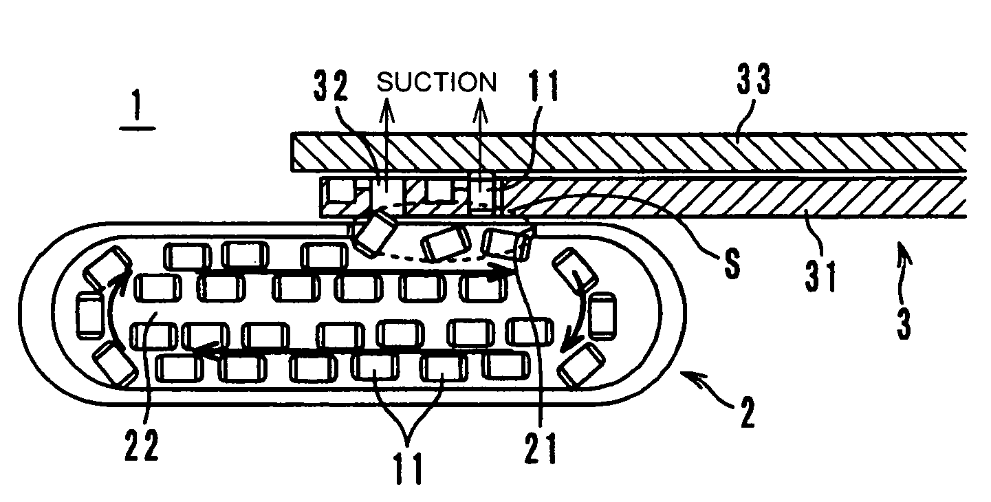
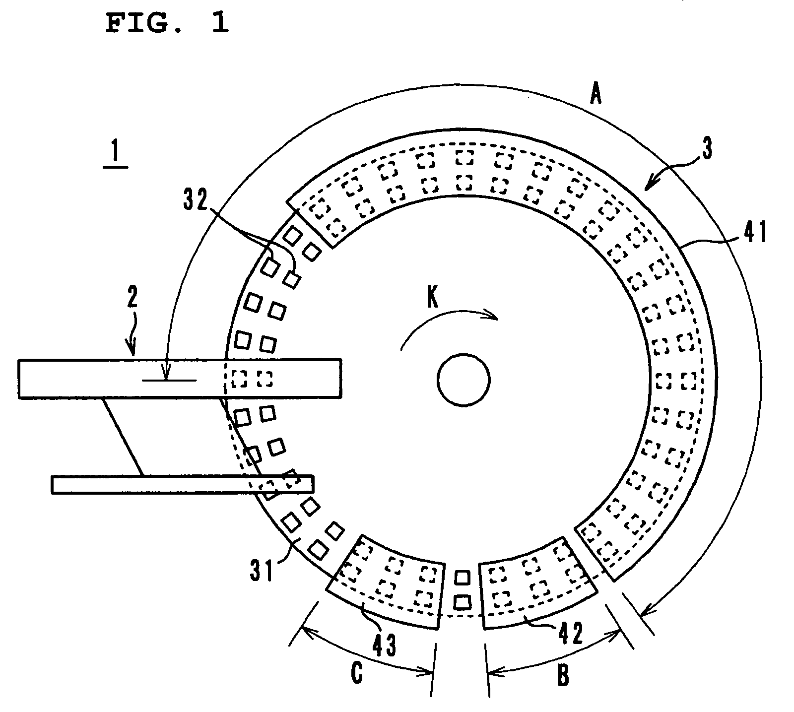
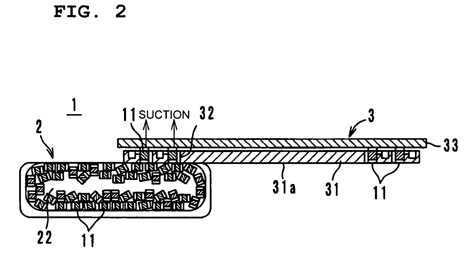
[0050]FIG. 1 is a front view of a handling device 1 for electronic chip components and FIG. 2 is a horizontal sectional view of the handling device 1. The handling device 1 for electronic chip components includes a circulatory feeder 2 (supplying feeder) and an indexing table 3 (accommodating device).

[0051]The circulatory feeder 2 includes a transport surface 22 having ...


PUM

PropertyMeasurementUnit
weightaaaaaaaaaa
lengthaaaaaaaaaa
suctionaaaaaaaaaa

Abstract

A handling device for electronic chip components includes an indexing table having a plurality of cavities for holding electronic chip components therein and a circulatory feeder for supplying the electronic chip components to the indexing table. One or more cavities are simultaneously disposed at a location which comes close to the circulatory feeder and, by performing a suction operation in the cavities, the electronic chip components are directly put into the cavities, without moving the electronic chip components along the main surface of the indexing table.

Description

BACKGROUND OF THE INVENTION[0001]1. Field of the Invention[0002]The present invention relates to a handling device for electronic chip components and a handling method for electronic chip components.[0003]2. Description of the Related Art[0004]A device for measuring electrical characteristics of electronic chip components such as chip capacitors, etc., and for screening conforming and nonconforming electronic chip components based on the measurements is described in PCT Japanese Translation Patent Publication No. 2000-501174.[0005]As shown in FIG. 23, such a device 101 contains a test plate 102 in which a plurality of holes (cavities) 103 is arranged along concentric circles for accommodating electronic chip components. A reduced pressure from a reduced pressure source is applied to each cavity 103 of the test plate 102 and, because of the suction generated by the reduced pressure, each cavity 103 sucks and holds a electronic chip component. Furthermore, the test plate 102 is inclin...

Claims


Application Information

Patent Timeline
Patent Type & Authority Patents(United States)
IPC IPC(8): B07C5/02B65G47/14B65G47/80H05K13/02
CPCH01L24/95H05K13/028H01L2924/01004H01L2924/01074H01L2924/01082H01L2924/19041H01L2924/19042G01R31/2893H01L2924/01005H01L2924/01006H01L2924/01019H01L2924/01033H01L2924/30105
Inventor TAKAGI, YUTAKAKARINO, EIJI
Owner MURATA MFG CO LTD
Why Eureka
Try Eureka