
Hybrid microwave integrated circuit

a hybrid microwave and integrated circuit technology, applied in the field of semiconductor amplifiers, can solve the problems of low power capability, unreliable and unreliable first semiconductor amplifiers, and devices tended to be leaky, and achieve the effect of less power capability

Active Publication Date: 2008-06-24
LOCKHEED MARTIN CORP
View PDF7 Cites 9 Cited by
  • Summary
  • Abstract
  • Description
  • Claims
  • Application Information

AI Technical Summary

Benefits of technology

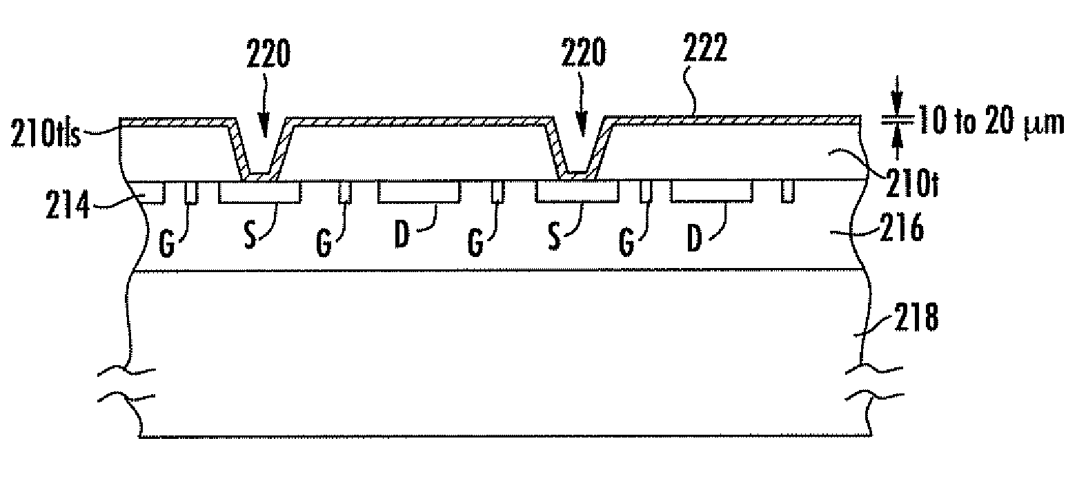
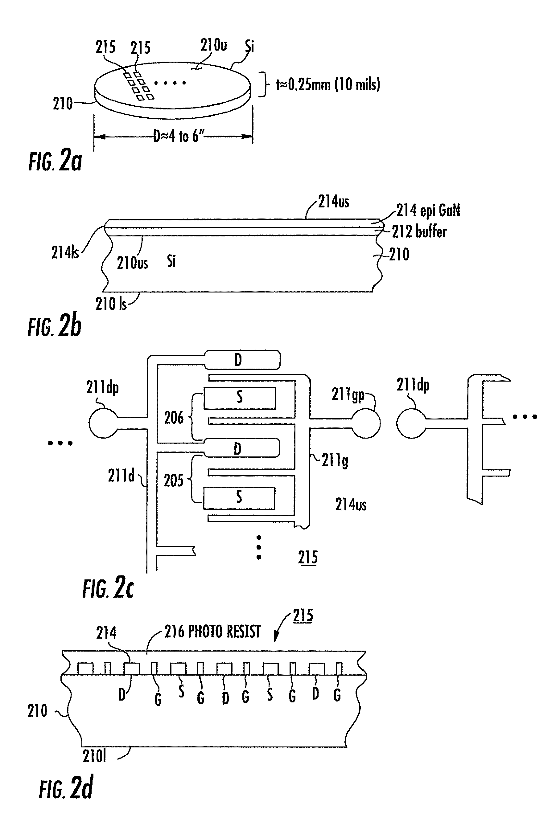
[0018]According to another aspect of the invention, an integrated-circuit amplifier for radio frequencies comprises a transistor sheet of a first semiconductor material, such as AlGaN/GaN, which has a first power capability. The sheet defines upper and lower sides, with the upper side being associated with at least one gate, drain and source portion. The sheet also defines a thickness between the upper and lower sides, which thickness is in the range of about 2 or 3 micrometers (μm), and also defines gate and drain ports associated with the upper side of the sheet. At least one of a gate matching circuit and a drain matching circuit are defined on a matching circuit substrate, which matching circuit substrate comprises a semiconductor material, such as GaAs, having lesser power capability, when used for a transistor, than the first semiconductor material. The matching circuit substrate defines upper and lower surfaces, and a thickness between the upper and lower surfaces, such as about 4 mils, which is substantially greater than that of the sheet. The matching circuit defines ports which are registered with the pattern of one of the gate and drain ports of the sheet when the one of the gate and drain ports of the sheet are juxtaposed with the ports of the matching circuit. A planar heat spreader substrate is made from one of an insulating and semi-insulating material, such as sapphire and Si, respectively, having thermal conductivity substantially less than that of the first semiconductor material. The heat spreader substrate defines first and second mutually parallel surfaces. The first of the mutually parallel surfaces of the heat spreader substrate is affixed to the l

Problems solved by technology

These devices tended to be leaky, in that unwanted current flows tended to upset the desired quiescent operating point, and they had relatively low voltage standoff capability, partially as a result of the tendency to leakage.
These combined to make the first semiconductor amplifiers little more than playthings, unreliable and with little power capability.
As an example of improvement in architecture, early transistors such as diffused transistors were three-dimensional, which tended to make heat removal difficult.
The inherent frequency limitations of early transistors, coupled with the unwanted stray reactances of the hard-wired circuits, sharply limited the high-frequency frequency response of amplifiers made with this technology.
The voltage and current limitations of the transistors also limited them to relatively low-power applications.
Unfortunately, such circuits tended to be hand-made, in that the transistors and other components were loaded by hand into printed circuit boards, and differences among the boards so produced led to significant performance differences among presumably identical units.
In addition to the problems there described, the type of semiconductor used for the common substrate tends to be driven by the requirements of the transistor portion.
However, the presence of matching circuits presents a challenge for MMICs.
Having conductor widths wider than the narrowest possible, however, tends to increase the surface area of the MMIC which is devoted to circuitry, which in turn leads to overall larger size, and to a requirement for more semiconductor material use.
On the other hand, very thin conductors can be lossy and difficult to define.
This, in turn, tends to make the design of the matching circuits difficult.
For example, Si has a much lower cost than GaAs, but a much lesser ultimate power capability.
Among the problems associated with these materials is reliability, which may be as low as 1000 hours mean time before failure (MTBF).
These problems may be related to lattice match dislocations between the semiconductor chips and the substrates on which they are mounted.
The development of monolithic microwave integrated circuits using SIC or GaN materials is proceeding, but it may be many years before reliable, high power MMICs are available using these technologies.
It is anticipated that this project may take several years to reach fruition, and it is conceivable that the desired result may never be achieved.

Method used


Image

  • Hybrid microwave integrated circuit
  • Hybrid microwave integrated circuit
  • Hybrid microwave integrated circuit

Examples


Embodiment Construction

[0025]The invention is based in part upon the understanding that a radio-frequency semiconductor amplifier has high capacitive impedance at its common-source input and output ports, and that the amount of power which can be produced into a nominal 50-ohm or 75-ohm load can be optimized over a given bandwidth by the use of input andor output matching filters or matching circuits. These filters are necessary for optimum performance, but need not be placed on the same semiconductor material as the transistor. The invention is also based in part upon an understanding that ideal microwave integrated circuit amplifier structures may not be achievable, or immediately achievable, and that compromises may be required to achieve the goal of high reliability, high power microwave integrated circuits.

[0026]GaN on Si substrates have demonstrated the potential to achieve power densities of 5 to 10 w / mm and higher with a MTBF of 1E6 hours. Silicon substrates are relatively desirable from a cost vi...


PUM


Abstract

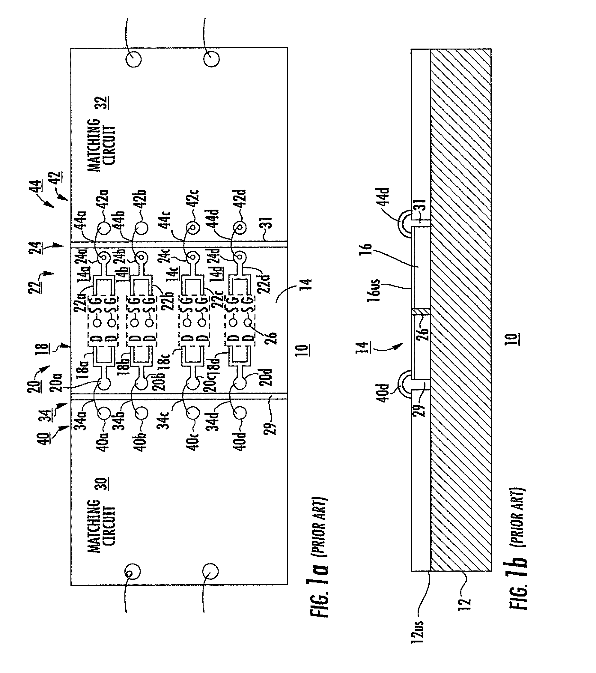
An integrated microwave transistor amplifier includes a AlGaN / GaN active transistor arrangement on a thinned Si 1-mil heat spreader. Elongated, plated-through vias extend from the source portions of the transistor arrangement through the spreader to a thick gold supporting layer. A matching circuit is defined on a four-mil GaAs substrate, also with a thick gold support layer. A stepped heat sink supports the matching circuit and the active transistor with surfaces coplanar. Bond wires interconnect the matching circuit with the gate or drain connections of the transistor.

Description

FIELD OF THE INVENTION[0001]This invention relates to semiconductor amplifiers for radio-frequency use, and more particularly to integrated structures using GaN or AlGaN transistors for high frequency, high power applications.BACKGROUND OF THE INVENTION[0002]There has been a long-felt need for semiconductor amplifiers for high-power radio-frequency applications. Those skilled in the art know that “radio” frequencies as now understood extends over the entire electromagnetic spectrum, including those frequencies in the “microwave” and “millimeter-wave” regions, and up to light-wave frequencies. Many of these frequencies are very important for commercial purposes, as they include the frequencies at which radar systems, global positioning systems, satellite cellular communications and ordinary terrestrial cellphone systems operate. Development of semiconductor devices to operate with significant power in some of these radio frequencies is extremely important in improving such services.[...

Claims


Application Information

Patent Timeline
IPC IPC(8): H01L29/80H01L31/112
CPCH01L23/36H01L23/66H01L27/0605H01L2223/6644H01L2224/48091H01L2224/49175H01L2924/01079H01L2924/10329H01L2924/14H01L2924/1423H01L2924/15153H01L2924/1517H01L2924/19041H01L2924/3011H01L2924/00014H01L2924/13063H01L24/48H01L24/49H01L2924/10253H01L2924/00H01L2924/30111H01L2224/45099H01L2224/45015H01L2924/207
Inventor KUMAR, MAHESH
Owner LOCKHEED MARTIN CORP
Learn More