Method and structure for implanting bonded substrates for electrical conductivity

a technology of electrical conductivity and substrate, which is applied in the manufacture of basic electric elements, semiconductor/solid-state devices, electrical apparatus, etc., can solve the problems of limiting the degree of integration of a given chip, conventional isolation techniques consume a considerable amount of valuable wafer surface area on the chip, and are not free from limitations, etc., to achieve improved process integration, high device yield, and convenient use

Active Publication Date: 2008-07-15
SILICON GENERAL CORPORATION
View PDF1 Cites 20 Cited by
  • Summary
  • Abstract
  • Description
  • Claims
  • Application Information

AI Technical Summary

Benefits of technology

[0013]Many benefits are achieved by way of the present invention over conventional techniques. For example, the present technique provides an easy to use process that relies upon conventional technology. In some embodiments, the method provides higher device yields. Additionally, the method provides a process that is compatible with conventional process technology without substantial modifications to conventional equipment and processes. Preferably, the invention provides for an improved process integration for advanced integrated circuit devices. Additionally, the process provides a multilayered substrate structure that includes electrical coupling between the first and second substrates. In a specific embodiment, the present method and structure can also reduce bond voids at the interface region between the two substrate members. The reduction of bond voids can occur by attaching one or more implanted particles to H / H2 atoms, which have been derived from a prior hydrogen treatment process as an example, that may be present at the interface region and may have contributed to formation of such voids at the interface region. Depending upon the embodiment, one or more of these benefits may be achieved. These and other benefits will be described in more throughout the present specification and more particularly below.

Problems solved by technology

These techniques, however, are not free from limitations.
For example, conventional isolation techniques consume a considerable amount of valuable wafer surface area on the chip, and often generate a non-planar surface as an artifact of the isolation process.
Either or both of these considerations generally limit the degree of integration achievable in a given chip.
Additionally, trench isolation often requires a process of reactive ion etching, which is extremely time consuming and can be difficult to achieve accurately.
Bulk silicon wafers, which are greater than 200 millimeters, are not free from defects and can reduce overall devices yields and the like.
Many problems, however, than have already been solved regarding fabricating devices on bulk silicon wafers remain to be solved for fabricating devices on epitaxial silicon wafers.
Epitaxial silicon wafers are made by way of epitaxial reactors, which are often expensive to purchase and difficult to maintain.
The process of forming epitaxial silicon is also slow and time consuming.
Accordingly, resulting epitaxial silicon wafers can often be expensive and cannot be used for the manufacture of many commercial or commodity devices such as dynamic random access memory devices (i.e., DRAMs), for example.
Although there has been much improvement in manufacturing substrate, there are still certain limitations that should be overcome.

Method used


Image

  • Method and structure for implanting bonded substrates for electrical conductivity
  • Method and structure for implanting bonded substrates for electrical conductivity
  • Method and structure for implanting bonded substrates for electrical conductivity

Examples


Embodiment Construction

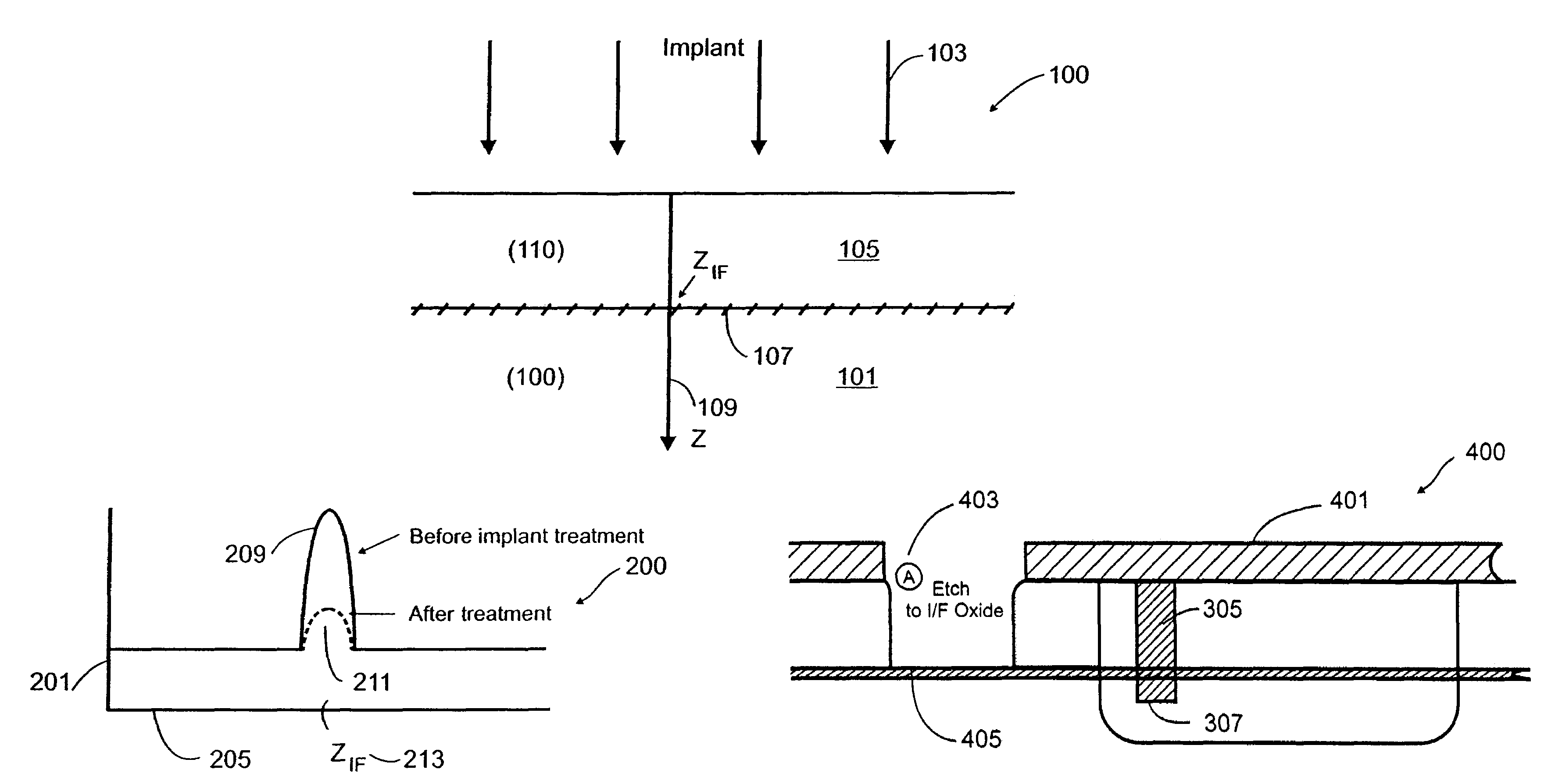
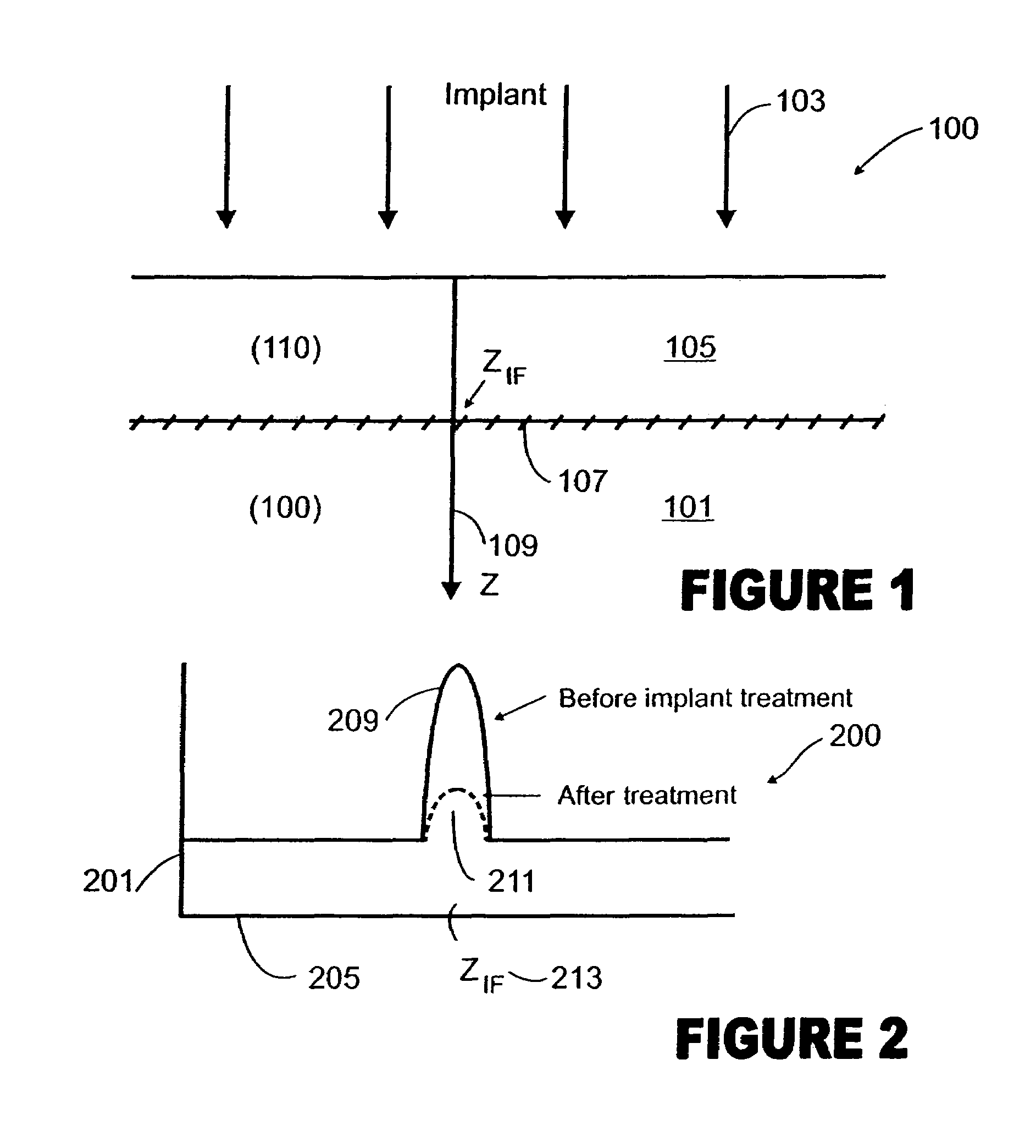
[0020]According to the present invention, techniques for the manufacture of substrates are provided. More particularly, the invention provides a technique including a method and device for forming a conductive region between bonded substrates using an implanting technique for the manufacture of semiconductor integrated circuits, for example. But it will be recognized that the invention has a wider range of applicability; it can also be applied to other substrates for multi-layered integrated circuit devices, three-dimensional packaging of integrated semiconductor devices, photonic devices, piezoelectronic devices, microelectromechanical systems (“MEMS”), sensors, actuators, solar cells, flat panel displays (e.g., LCD, AMLCD), biological and biomedical devices, and the like.

[0021]A method for manufacturing bonded substrates according to an embodiment of the present invention may be outlined as follows:

[0022]1. Provide a first substrate, which has a thickness of material to be removed...


PUM

PropertyMeasurementUnit
thicknessaaaaaaaaaa
temperatureaaaaaaaaaa
thicknessaaaaaaaaaa

Abstract

A partially completed multi-layered substrate, e.g., silicon on silicon. The substrate has a thickness of material from a first substrate. The thickness of material comprises a first face region. The substrate has a second substrate having a second face region. Preferably, the first face region of the thickness of material is joined to the second face region of the second substrate. The substrate has an interface region formed between the first face region of the thickness of material and the second face region of the second substrate. A plurality of particles are implanted within a portion of the thickness of the material and a portion of the interface region to electrically couple a portion of the thickness of material to a portion of the second substrate.

Description

CROSS-REFERENCE TO RELATED APPLICATIONS[0001]This application is continuation-in-part of, and claims priority to, U.S. Nonprovisional patent application Ser. No. 11 / 280,016 filed on Nov. 15, 2005, which claims priority to U.S. Provisional Patent Application 60 / 630,800 filed Nov. 24, 2004, each of which is commonly assigned, and each of which is hereby incorporated by reference for all purposes.BACKGROUND OF THE INVENTION[0002]The present invention relates to the manufacture of substrates. More particularly, the invention provides a technique including a method and device for forming a conductive region between bonded substrates using an implanting technique for the manufacture of semiconductor integrated circuits, for example. But it will be recognized that the invention has a wider range of applicability; it can also be applied to other substrates for multi-layered integrated circuit devices, three-dimensional packaging of integrated semiconductor devices, photonic devices, piezoel...

Claims


Application Information

Patent Timeline
Patent Type & Authority Patents(United States)
IPC IPC(8): H01L21/30H01L21/46
CPCH01L21/26513
Inventor HENLEY, FRANCOIS J.
Owner SILICON GENERAL CORPORATION
Why Eureka
Try Eureka