Organic electroluminescence device with absorbent film and fabrication method thereof

a technology of organic electroluminescence and absorbent film, which is applied in the field of display devices, can solve the problems of organic electroluminescence devices determined as failures, limited total yield, and deterioration of organic electroluminescence devices according to the related art, so as to improve durability and impact resistance stability, improve device life, and improve device life

Active Publication Date: 2008-07-22
LG DISPLAY CO LTD
View PDF11 Cites 26 Cited by
  • Summary
  • Abstract
  • Description
  • Claims
  • Application Information

AI Technical Summary

Benefits of technology

[0020]An object of the present invention is to provide an organic electro luminescence device and a fabrication method thereof that has an absorbent provided within an array of an upper substrate or a lower substrate of the organic electro luminescence device to eliminate internal moisture from the organic electro luminescence device, thereby improving a device life and improving a durability and an impact-resistance stability.
[0021]Another object of the present invention is to provide a pattern structure and a method of fabricating the same that provide an organic electro luminescence device and a fabrication method thereof in which a thin layer is formed with a predetermined pattern and an absorption function, within an array and at an outer part of the upper substrate or the lower substrate of the organic electro luminescence device, to eliminate internal moisture from the organic electro luminescence device, thereby improving a device life and improving a durability and an impact-resistance stability.

Problems solved by technology

However, the organic electro luminescence device according to the related art has a drawback.
Since a yield of the array device is multiplied by a yield of the organic electro luminescence diode to determine an overall yield of the organic electro luminescence device, a total yield is greatly limited by a fabrication process of an organic electro luminescence diode.
For example, even if the array device is formed with a good quality, the organic electro luminescence device is determined as a failure when the organic electro luminescence layer having a thickness of about 1000 Å is degraded due to a foreign material.
As a result, the process and material costs in fabricating the good array device is wasted, and an overall production yield is decreased.
In addition, the bottom emission type device has a limited aperture ratio, thereby limiting its application in high-resolution displays.
However, since the top emission type device generally has the cathode electrode disposed on the organic electro luminescence layer, there are limited choices in material for forming the cathode electrode.
Thus, the transmittance of the top emission type device is limited by this narrow material selection range, thereby reducing light efficiency.
Further, when a thin film type passivation film is used for minimizing a reduction in the light transmittance, external air is not sufficiently cut off from the interior of the top emission type device.
Moreover, a problem exists in placing a desiccant in a top emission type device because the array device and the organic electro luminescence layer are formed on different substrates.

Method used


Image

  • Organic electroluminescence device with absorbent film and fabrication method thereof
  • Organic electroluminescence device with absorbent film and fabrication method thereof
  • Organic electroluminescence device with absorbent film and fabrication method thereof

Examples


Embodiment Construction

[0040]Reference will now be made in detail to the preferred embodiments, examples of which are illustrated in the accompanying drawings.

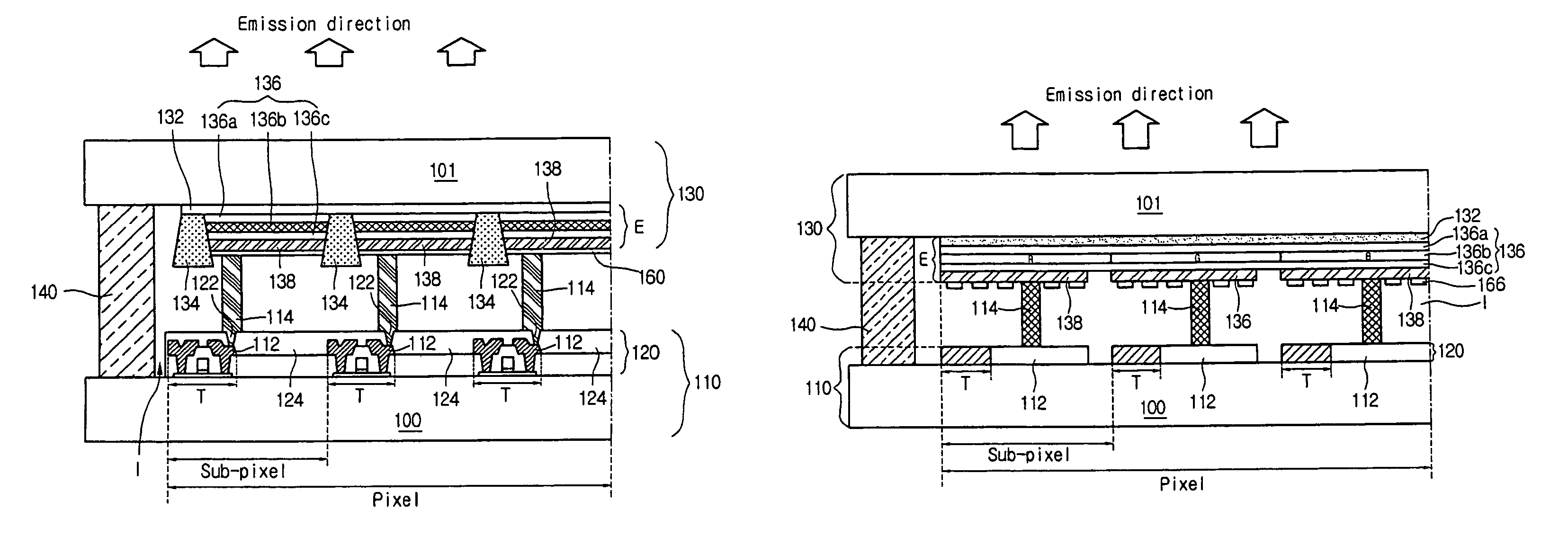
[0041]FIG. 5 is a schematic sectional view of a dual panel type organic electro luminescence device according to an embodiment of the present invention. In FIG. 5, an organic electro luminescence device may include first and second substrates 110 and 130 attached to each other by a seal pattern 140 with a predetermined distance therebetween. An array device 120 may be formed on a first transparent substrate 100 of the first substrate 110, and an organic electro luminescence diode E may be formed on a second transparent substrate 101 of the second substrate 130.

[0042]The organic electro luminescence diode E may include a first electrode 132 as a common electrode, barriers 134 corresponding to a boundary of sub-pixel regions, and an organic electro luminescence layer 136 and a second electrode 138 sequentially formed between the barriers 134 correspon...


PUM


Abstract

An organic electro luminescence device includes an array device having a thin film transistor formed in each of sub-pixel regions on a first substrate, a first electrode of an organic electro luminescence diode formed on a second substrate, the first electrode including a metallic material having light transmittance, a second electrode and an organic electro luminescence layer of the organic electro luminescence diode formed on the first electrode, and a thin film type absorbent formed on one of the first substrate and the second substrate, the first and second substrates being attached to each other with a predetermined distance therebetween having the array device facing the organic electro luminescence diode, and including a conductive spacer for electrically connecting the thin film transistor and the second electrode.

Description

[0001]The present application claims the benefit of Korean Patent Application No. 85398 / 2003 filed in Korea on Nov. 28, 2003 and Korean Patent Application No. 85399 / 2003 filed in Korea on Nov. 28, 2003, which are hereby incorporated by reference.BACKGROUND OF THE INVENTION[0002]1. Field of the Invention[0003]The present invention relates to a display device, and more particularly, to a dual panel type organic electroluminescence device and method for fabricating the same.[0004]2. Discussion of the Related Art[0005]In general, an organic electro luminescence device, which also is referred to as an organic light emitting diode (OLED) device, is a self-emission type display and includes a plurality of pixels and an organic light emitting diode in each of the pixels. Each of the organic light emitting diodes emits light by injecting electrons from a cathode and holes from an anode into an emission layer, combining the electrons with the holes, generating an exciton, and transitioning th...

Claims


Application Information

Patent Timeline
Patent Type & Authority Patents(United States)
IPC IPC(8): H01J1/62H01J63/04G09F9/30H05B33/04H01L27/32H01L51/50H01L51/52H05B33/10H05B33/12H05B33/14H05B33/22H05B33/26
CPCH01L51/5237H01L27/3251H10K59/127H10K59/874H10K50/846
Inventor PARK, JAE YONGLEE, NAM YANGKIM, KWAN SOO
Owner LG DISPLAY CO LTD
Why Eureka
Try Eureka