Light modulation information display device and illumination control device

Inactive Publication Date: 2005-10-18
SHARP KK
View PDF6 Cites 21 Cited by
  • Summary
  • Abstract
  • Description
  • Claims
  • Application Information

AI Technical Summary

Benefits of technology

[0057]As a result, it is possible to prevent an increase in the number of times a discharge starting voltage is applied, which may occur when flickering, i.e., repetitions of a complete OFF state and a complete ON (entire discharging) state is performed (as in a conventional illumination device which has been proposed for improving display blurs associated with line-of-sight tracing). Thus, drastic reduction in the device life of the illumination devices (fluorescence discharge tubes) can be prevented.
[0058]Furthermore, the length of the illumination device is designed so as to be greater than the corresponding dimension of the effective display area of an LM information display section and the corresponding dimension of a light guide layer which is provided on a front face or back face of the LM information display section, and an activation control section for controlling the illumination devices may be provided on a front face or a back face of the portion of the illumination device which protrudes outside the effective display area of the LM information display section and the light guide layer. As a result, the entire LM information display device can be prevented from having an increased structure size.
[0059]According to the present invention, the illumination control device is operated so as to provide an entirely-ON period during which an entirely-ON voltage for causing the illumination device to be turned entirely-ON is applied between two main discharging electrodes of the illumination device, a partially-ON period during which a partially-ON voltage for turning ON only a portion of the illumination device is applied between at least one of the main discharging electrodes and a neighboring partial discharging electrode, or a partial discharging period during which a partially discharging voltag

Problems solved by technology

Firstly, an increase in the power consumption in the liquid crystal display device results, thereby detracting from its comparative advantages over other types of display devices (CRTs, PDPs (plasma display panels), etc.).
Secondly, since there is an increased number of fluorescence discharge tubes with a high density, the temperature of the fluorescence discharge tubes may increase as a result of controlling the fluorescence discharge tubes so as to be always ON, resulting in a decrease in display contrast.
Thirdly, there is a problem associated with the response speed, which is dependent on the particular liquid crystal material used: outstanding display blurs (e.g., blurred outlines) and residual images will occur when moving pictures are displayed at a fast rate.
It is known that, since the amount of electrons which are sputtered increases at the beginning of the discharging, vigorous sputtering occurs in the neighborhood of the electrodes, leading to the blackening of the fluorescent material and the deterioration of the electrodes.
While the aforementioned technique of repeatedly turning ON or OFF the fluorescence discharge tubes as illustrated in Conventional Example 1 does contribute to an improvement in power consumption, it is disadvantageous in terms of the device life of the fluorescence discharge tubes.
Consequently, excessive components may be applied to the fluorescence discharge tubes as a discharge startin

Method used


Image

  • Light modulation information display device and illumination control device
  • Light modulation information display device and illumination control device
  • Light modulation information display device and illumination control device

Examples


example 1

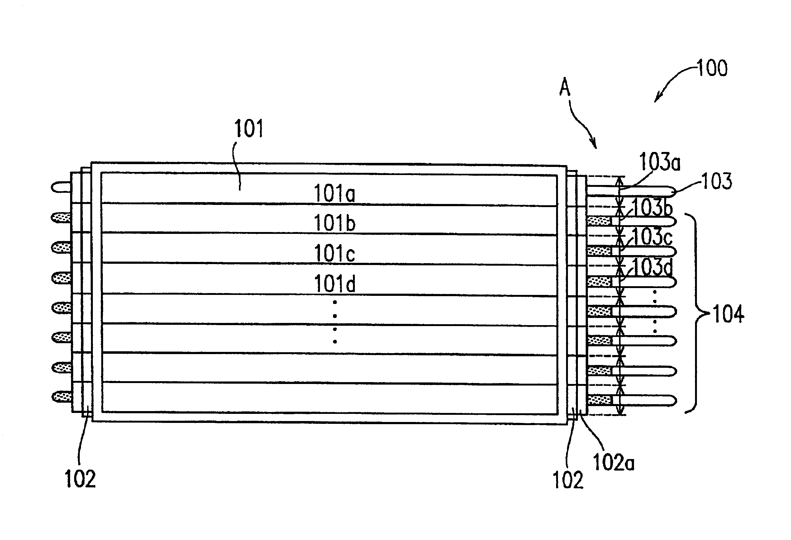
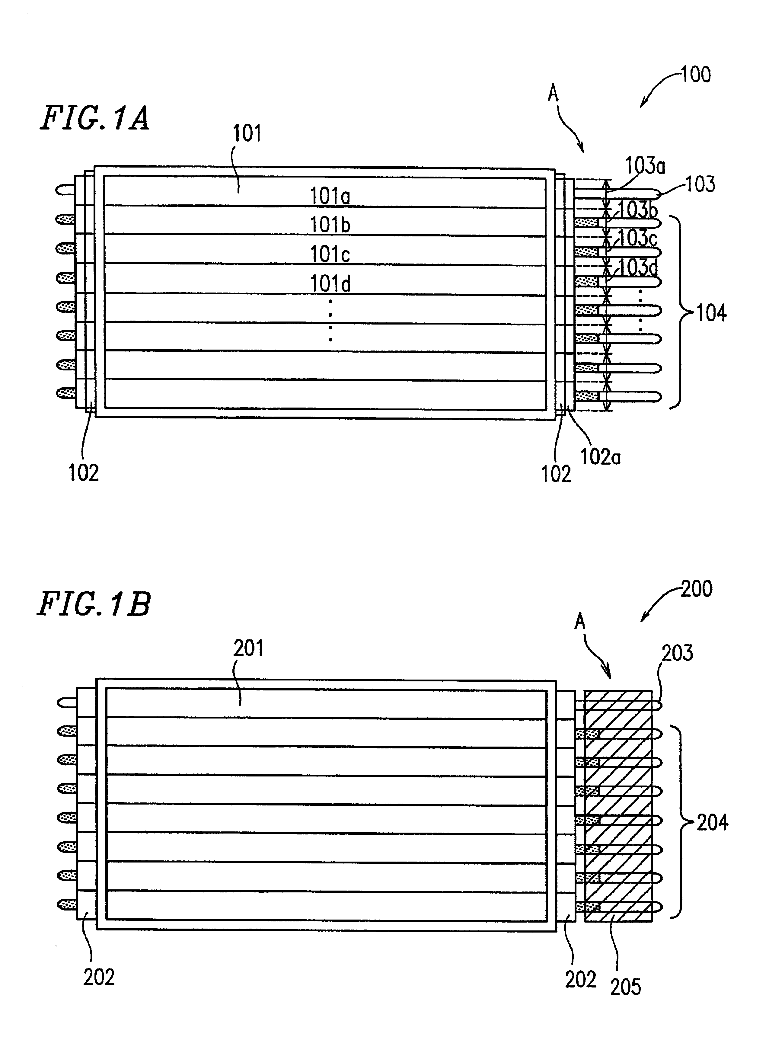
[0091]FIG. 1A is a plan view schematically illustrating an underlying-type backlight LM information display device 100 according to Example 1 of the present invention.

[0092]The LM information display device 100 includes an LM information display section 101, illumination devices 103 and 104, and a light guide layer 102 which is provided on a back face of the LM information display section 101 for guiding the illumination light emitted from the illumination devices 103 and 104 into the LM information display section 101. The illumination devices 103 and 104 are provided directly under the light guide layer 102. The illumination devices 103 and 104 are controlled by an illumination control device which is described later.

[0093]In the present example, a liquid crystal panel including TFTs (thin film transistors) serving as light-switching elements is used for the LM information display section 101. As the light guide layer 102, a colorless plate of acrylic resin may be used, and a diff...

example 2

[0116]FIG. 6 is a plan view schematically illustrating a side-type backlight LM information display device 600 according to Example 2 of the present invention.

[0117]The side-type backlight LM information display device 600 includes an LM information display section 611, a light guide layer 612 for guiding light into the LM information display section 611, a lamp reflector 606a for deflecting light toward the light guide layer 612, and at least one fluorescence discharge tube 606 which is partially surrounded by the lamp reflector 606a. Although the illumination devices (the fluorescence discharge tubes 606) in the LM information display device 600 of FIG. 6 are disposed perpendicularly to the horizontal scanning lines of the LM information display section 611, illumination devices may alternatively be provided in parallel to the horizontal scanning lines. The fluorescence discharge tube(s) 606 and the lamp reflector(s) 606a do not need to be provided on both sides of the light guide...

example 3

[0144]FIG. 13 is a block diagram schematically illustrating an illumination control device 1300 according to Example 3 of the present invention.

[0145]The illumination control device 1300 includes a cold-cathode fluorescence discharge tube 1301, an electrode selection circuit 1302, an inverter circuit 1303, a driving waveform generation section 1304, and an activation synchronization signal generation circuit 1305.

[0146]The diameter and tube length of the cold-cathode fluorescence discharge tube 1301 are diameter φ=2.6 and 400 mm, respectively. A fluorescent material is applied to the inner surface of the cold-cathode fluorescence discharge tube 1301. The total gas pressure within the cold-cathode fluorescence discharge tube 1301 is 60 Torr. Ag and Hg are contained within the fluorescence discharge tube 1301 as main gas components. The cold-cathode fluorescence discharge tube 1301 includes main discharging electrodes 1301x and 1301y provided on both ends thereof for turning the fluor...


PUM


Abstract

An illumination control device for illuminating an light modulation information display device with light includes: at least one illumination device for irradiating light which is generated through discharging; and a driving waveform generation section for controlling the light which is irradiated from the at least one illumination device to the light modulation information display device. The light modulation information display device is operable so as to have a first period and a second period during which an image is displayed. During the first period, the driving waveform generation section applies a first voltage to the at least one illumination device, the first voltage causing the at least one illumination device to be turned entirely-ON. During the second period, the driving waveform generation section applies a second voltage to at least a portion of the at least one illumination device.

Description

BACKGROUND OF THE INVENTION[0001]1. Field of the Invention[0002]The present invention relates to a light modulation information display device (hereinafter referred to as an “LM information display device”) which displays information through variable control of the transmission, absorption, interception, reflection state or reflection direction of light, and an illumination control device for controlling an illumination device which is provided on a back face or a front face of a display section of an LM information display device. In particular, the present invention relates to an LM information display device and an illumination control device which can provide improved power consumption and improved display quality for moving pictures, and higher reliability. Moreover, the present invention relates particularly to: an LM information display device which can be suitably used as a liquid crystal display device for displaying moving pictures or the like; and an illumination control ...

Claims


Application Information

Patent Timeline
IPC IPC(8): G09G3/34
CPCG09G3/342G09G2310/024G09G2310/08H01J61/025H01J61/70H01J61/92
Inventor KYOMOTO, TADAO
Owner SHARP KK
Why Eureka
Try Eureka