

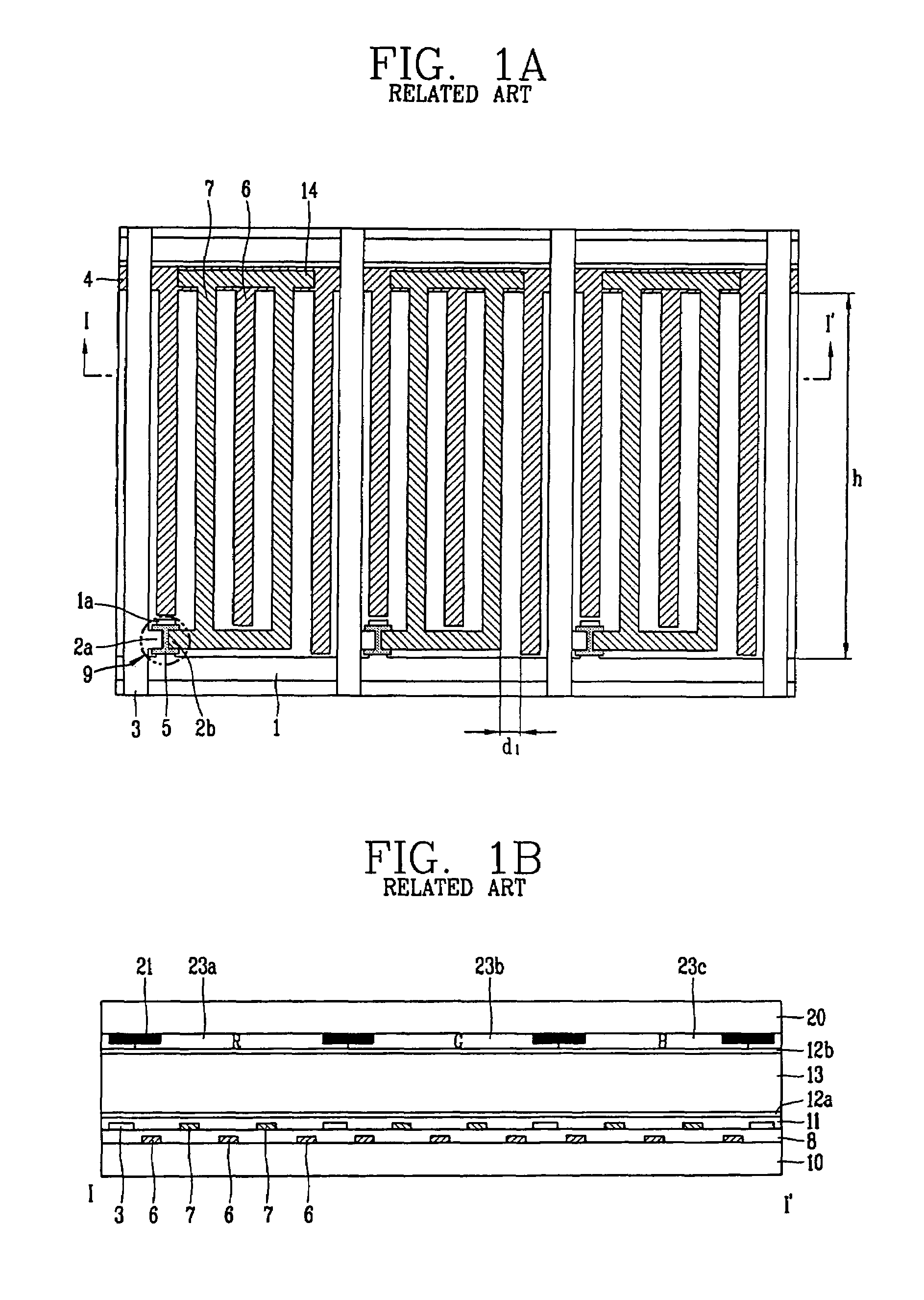
Plane switching mode liquid crystal display device having storage lines overlapping gate line and common line, and fabrication method thereof
a liquid crystal display device and plane switching technology, applied in optics, instruments, electrical appliances, etc., can solve the problems of reducing the aperture ratio, narrow viewing angle, degrading brightness, etc., to achieve the effect of improving the aperture ratio, improving the brightness of the screen, and easily controlling the area of sub-pixels
- Summary
- Abstract
- Description
- Claims
- Application Information
AI Technical Summary
Benefits of technology
Problems solved by technology
Method used
Image

Examples
first embodiment
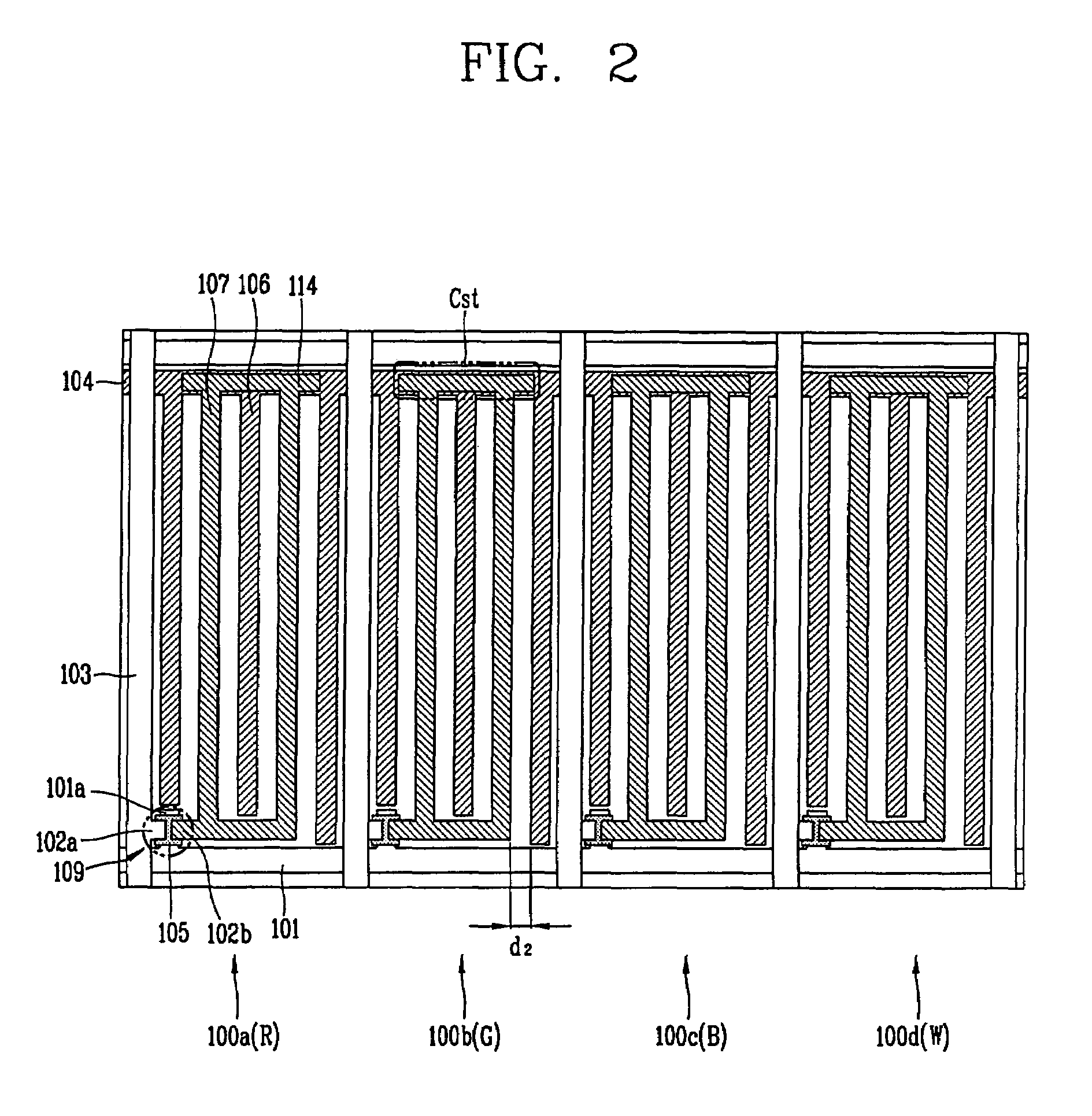
[0032]FIG. 2 illustrates the present invention: an in plane switching (IPS) mode liquid crystal display (LCD) device having four sub-pixels, wherein each sub-pixel has four transmissive regions. This embodiment of the IPS mode LCD device has a white sub-pixel 100d in addition to the Red 100a, Green 100b and Blue 100c sub-pixels. Here, the W sub-pixel 100d may be accommodated by reducing the width of each sub-pixel and maintaining each sub-pixel's area.
[0033]The sub-pixels 100a, 100b, 100c and 100d are defined by a gate lines 101 and a data lines 103 arranged horizontally and vertically. In each sub-pixel 100a, 100b, 100c, 100d, a pixel electrode 107 substantially perpendicularly connects to a pixel electrode line 114, and a common electrode 106 substantially perpendicularly connects to a common line 104. The pixel electrode 107 and the common electrode 106, which are alternately disposed, generate an in-plane electric field in the pixel when a voltage is applied between them. In add...
second embodiment
[0036]FIG. 3 illustrates a second exemplary embodiment of the present invention. In the second embodiment, sub-pixels R, G, B and W are arranged in a 2×2 matrix form, and each sub-pixel has six transmissive regions between electrodes 206 and 207, wherein each transmissive region that has a width, D1, that is substantially the same as the corresponding width of the related art structure. The sub-pixel arrangement, and the width of the transmission region, D1, improve brightness and aperture ratio relative to the related art.
[0037]As illustrated in FIG. 3, the IPS mode LCD device according to the second embodiment has R, G, B and W sub-pixels 200a-200d, each having six transmissive regions, wherein the sub-pixels are arranged in the 2×2 matrix to form a unit pixel (P). The sub-pixels 200a-200d are defined by gate lines 201 and data lines 203, respectively, and are arranged horizontally and vertically. In each sub-pixel 200a-200d is at least one pair of electrodes, a pair including a p...
third embodiment
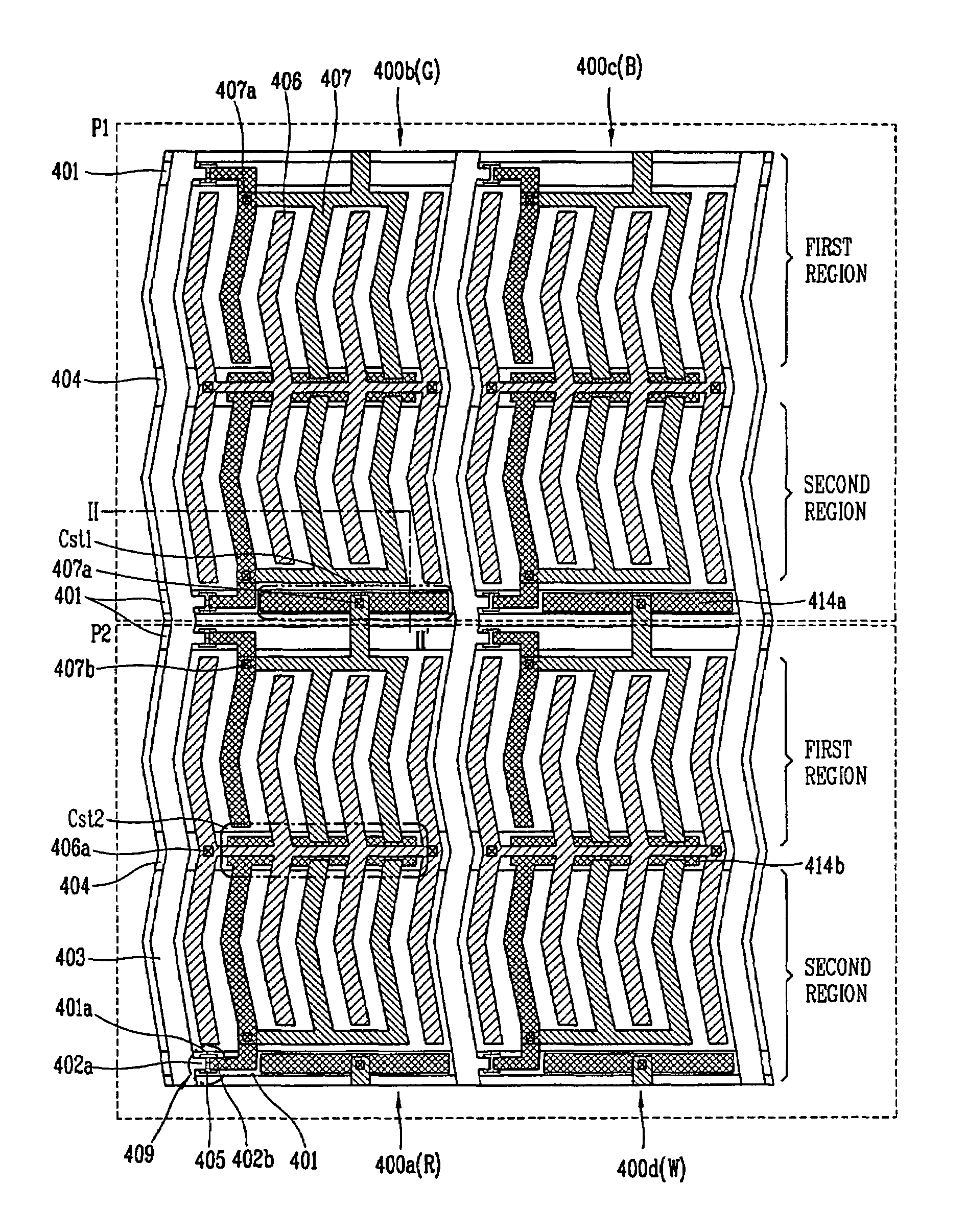
[0042]As illustrated in FIG. 4, in the IPS mode LCD device a unit pixel is divided into sub-pixels by a common line 304 passing through a center of the pixel (P) parallel to a gate line 301, and R, G, B and W sub-pixels 300a-300d are arranged in a 2×2 matrix form. The region above the common line 304 may be referred to as a first region, and the region below the common line 304 may be referred to as a second region. As illustrated in FIG. 4, the G and B sub-pixels 300b and 300c are disposed in the first region, and R and W sub-pixels 300a and 300d are disposed in the second region.
[0043]The common line 304 is electrically connected to at least one common electrode 306 disposed in each sub-pixel, and forms a storage capacitor (Cst) together with a pixel electrode line 314 overlapping the common line 304. As illustrated in FIG. 4, the pixel electrode line 314 overlapping the common line 304 includes a first pixel electrode line 314a electrically connected to a pixel electrode 307 for...
PUM
| Property | Measurement | Unit |
|---|---|---|
| transparent | aaaaa | aaaaa |
| zigzag structure | aaaaa | aaaaa |
| structure | aaaaa | aaaaa |
Abstract
Description
Claims
Application Information