Supercharge Your Innovation With Domain-Expert AI Agents!

CMOS image sensor and method for manufacturing the same

a metal oxidesemiconductor and image sensor technology, applied in the direction of diodes, semiconductor devices, radiation control devices, etc., can solve the problems of degrading color reproduction quality, blue photodiodes that cannot sense shorter wavelengths, etc., to improve blue light sensitivity and thickness. , the effect of increasing the thickness

Inactive Publication Date: 2008-07-29
DONGBU ELECTRONICS CO LTD
View PDF5 Cites 0 Cited by
  • Summary
  • Abstract
  • Description
  • Claims
  • Application Information

AI Technical Summary

Benefits of technology

This design improves blue light sensitivity and color reproduction by increasing the effective thickness of the blue photodiode region, enabling better capture of blue wavelengths and enhancing overall image quality.

Problems solved by technology

In the related art CMOS image sensor manufactured above, however, the blue photodiode may fail to sense shorter wavelengths because blue light in a general pixel structure has a penetration depth of 0.3 μm.
Therefore, the desired display of the respective colors (i.e., red, green, and blue) at a ratio of 1:1 is impeded, thereby degrading color reproduction quality.

Method used


Image

  • CMOS image sensor and method for manufacturing the same
  • CMOS image sensor and method for manufacturing the same
  • CMOS image sensor and method for manufacturing the same

Examples


Embodiment Construction

[0030]Reference will now be made in detail to embodiments of the present invention, examples of which are illustrated in the accompanying drawings. Wherever possible, like reference designations will be used throughout the drawings to refer to the same or similar parts.

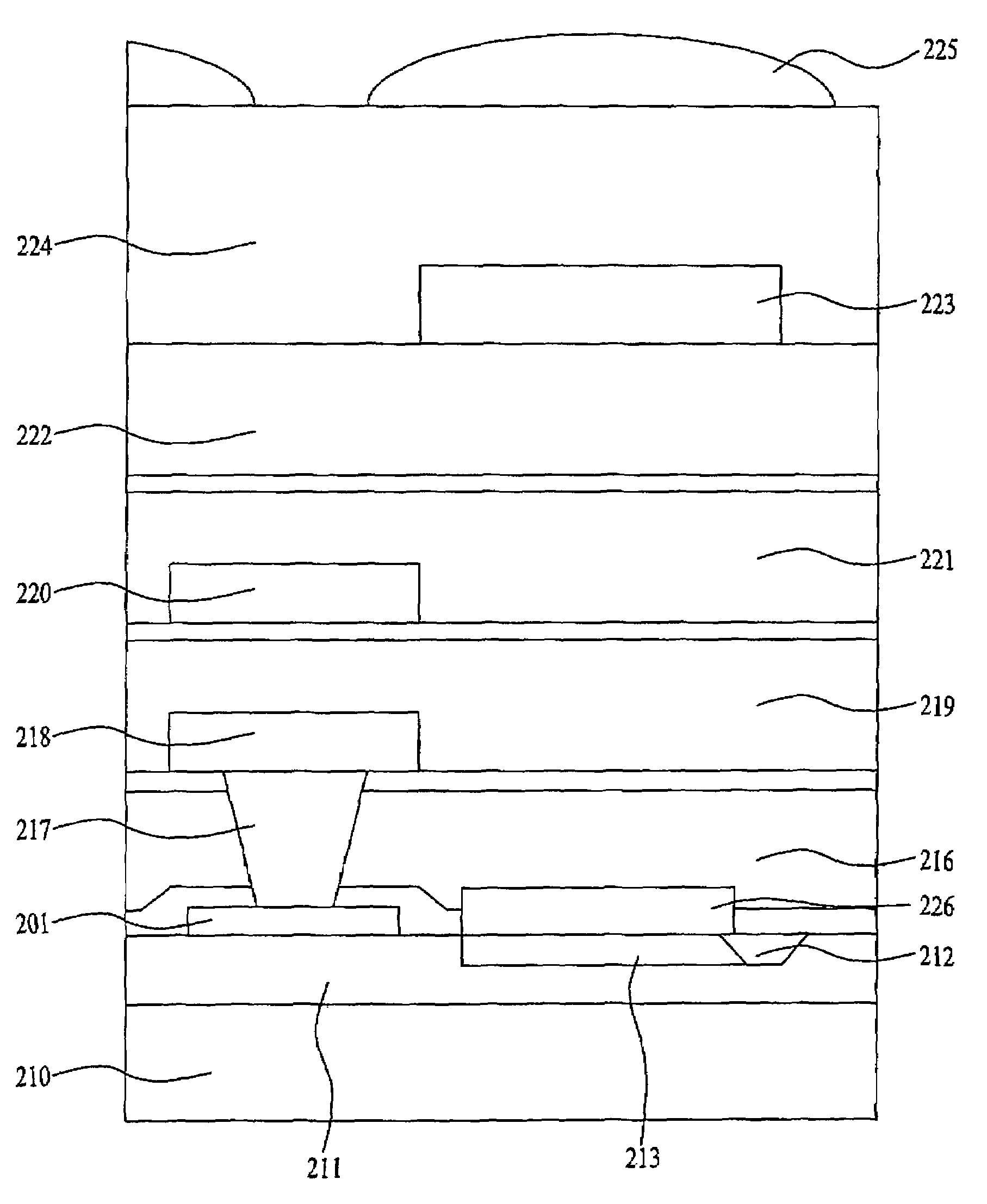
[0031]Referring to FIG. 4, illustrating a blue photodiode portion of a CMOS image sensor according to the present invention, a device isolation film 212 is formed on a semiconductor substrate 210 in which a first lightly doped P-type epitaxial layer 211 is formed. The device isolation film 212 serves to isolate an active region including a lightly doped N-type blue photodiode region 213. A second lightly doped N-type epitaxial layer 226 is formed on the photodiode region 213.

[0032]A transfer transistor 201 including a gate electrode is formed on the first epitaxial layer 211. A first interlayer dielectric film 216 is formed on the first epitaxial layer 211 including the transfer transistor 201. The first interlayer di...


PUM


Abstract

A CMOS image sensor and a method for manufacturing the same are disclosed, in which a blue photodiode is imparted with a greater thickness to improve sensitivity of blue light. The blue photodiode of a CMOS image sensor includes a first lightly doped P-type epitaxial layer formed on a heavily doped P-type semiconductor substrate; a gate electrode of a transfer transistor formed on the first epitaxial layer; a first N-type blue photodiode region formed on the first epitaxial layer; and a second N-type blue photodiode region formed on the first epitaxial layer corresponding to the first blue photodiode region.

Description

[0001]This application claims the benefit of Korean Patent Application No. 10-2004-0116423, filed on Dec. 30, 2004, which is hereby incorporated by reference for all purposes as if fully set forth herein.BACKGROUND OF THE INVENTION[0002]1. Field of the Invention[0003]The present invention relates to complementary metal-oxide-semiconductor (CMOS) image sensors, and more particularly, to a blue photodiode of a CMOS image sensor and a method for manufacturing the same, in which the blue photodiode is formed to be higher and wider than a semiconductor substrate to improve sensitivity of blue light.[0004]2. Discussion of the Related Art[0005]An image sensor is a semiconductor device that converts optical images to electrical signals. The image sensor is classified into a charge-coupled device (CCD) and a CMOS image sensor. The CCD stores charge carriers in MOS capacitors and transfers the charge carriers to the MOS capacitors. The MOS capacitors are approximate to one another. The CMOS i...

Claims


Application Information

Patent Timeline
Patent Type & Authority Patents(United States)
IPC IPC(8): H01L21/00
CPCH01L27/14689H01L27/14643H01L27/146H01L31/10
Inventor HAN, CHANG HUN
Owner DONGBU ELECTRONICS CO LTD
Features
  • R&D
  • Intellectual Property
  • Life Sciences
  • Materials
  • Tech Scout
  • Unparalleled Data Quality
  • Higher Quality Content
  • 60% Fewer Hallucinations
Learn More