Plastic package and method of fabricating the same

a plastic package and plastic technology, applied in the direction of semiconductor devices, electrical equipment, semiconductor/solid-state device details, etc., can solve the problems of difficult to reduce the thickness of the plastic package, high development cost and long development time, and the inability to achieve one-chip system lsi, etc., to achieve efficient mass production and reliable connection

Active Publication Date: 2008-07-29
DAI NIPPON PRINTING CO LTD
View PDF4 Cites 24 Cited by
  • Summary
  • Abstract
  • Description
  • Claims
  • Application Information

AI Technical Summary

Benefits of technology

[0013]The present invention has been made to meet the foregoing requirements and it is therefore an object of the present invention to provide a package capable of further reducing the thickness of a semiconductor device at a low cost. More concretely, the present invention provides a stacked, plastic package realizing a stacked system package built by stacking a plurality of plastic packages. Thus, the present invention provides an easily mass-producible plastic package.
[0014]Another object of the present invention is to provide an easily mass-producible semiconductor device suitable for achieving the further reduction of the thickness of a semiconductor part at a low cost. A third object of the present invention is to provide a stacked plastic package built by stacking such thin plastic packages and realizing the so-called stacked system package.

Problems solved by technology

Two-dimensional wiring limits increasing operating speed by shortening wiring lines, and the development of techniques to achieve one-chip system LSI requires high development costs and long development time.
However, those plastic packages are provided with a die pad and hence it is difficult to reduce the thickness of those plastic packages.
This package has low application flexibility and is difficult to apply to general purposes.

Method used


Image

  • Plastic package and method of fabricating the same
  • Plastic package and method of fabricating the same
  • Plastic package and method of fabricating the same

Examples


first embodiment

[0118]Preferred embodiments of the present invention will be described with reference to the accompanying drawings.

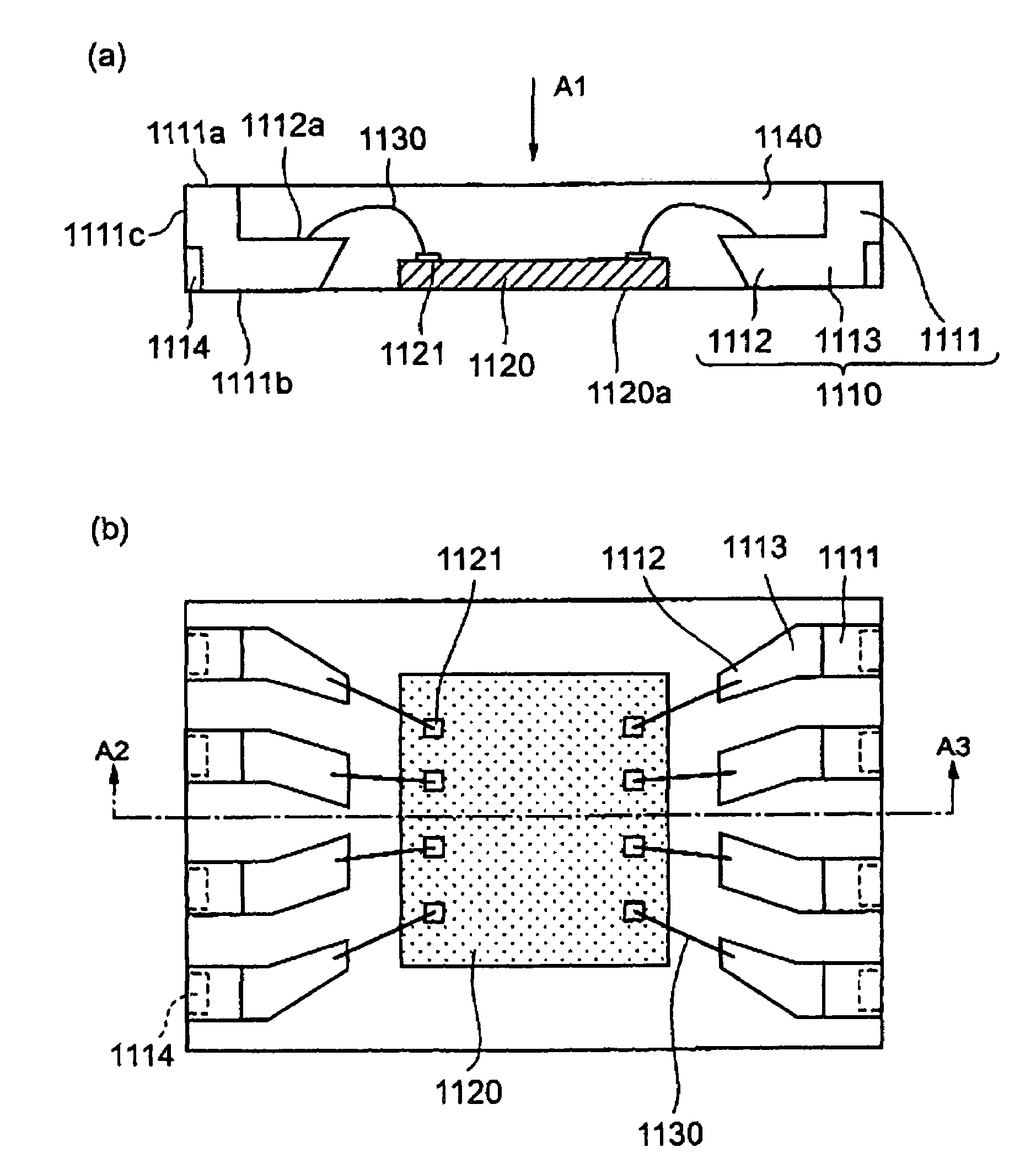
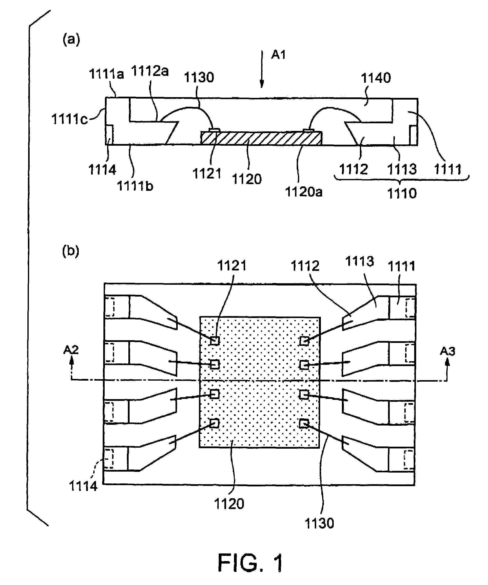
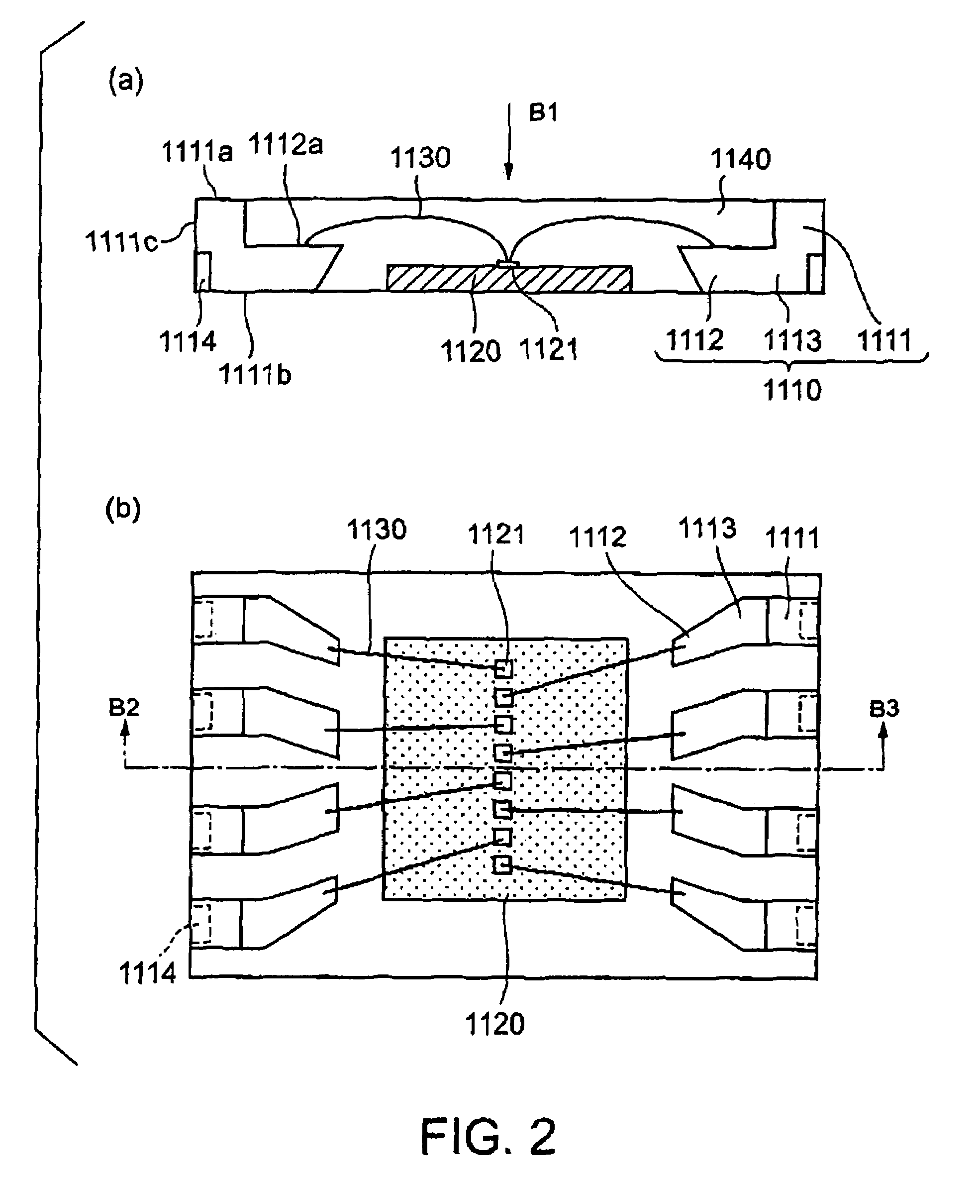
[0119]FIG. 1(a) is a partly sectional side elevation of a plastic package in a first example of a first embodiment according to the present invention , FIG. 1(b) is a view taken in the direction of the arrow A1 in FIG. 1(a), FIG. 2(a) is a partly sectional side elevation of a plastic package in a second example of the first embodiment, FIG. 2(b) is a view taken in the direction of the arrow B1 in FIG. 2(a), FIG. 3 illustrates steps of a plastic package fabricating method in a first example according to the present invention, FIG. 4 illustrates steps of a plastic package fabricating method in a second example according to the present invention, FIG. 5 is a sectional view of a stacked plastic package in a first example, FIG. 6 is a sectional view of a stacked plastic package in a second example, FIG. 7 is a sectional view of a stacked plastic package in a third example, F...

second embodiment

[0183]A second embodiment of the present invention will be described.

[0184]FIG. 11(a) is a sectional view of a plastic package in a first example of a second embodiment according to the present invention , FIG. 11(b) is a view taken in the direction of the arrow A1 in FIG. 11(a), FIG. 12(a) is a sectional view of a plastic package in a second example of the second embodiment, FIG. 12(b) is a view taken in the direction of the arrow B1 in FIG. 12(a), FIG. 13(a) is a sectional view of a plastic package in a third example of the second embodiment, FIG. 13(b) is a view take in the direction of the arrow C1 in FIG. 13(a), FIG. 14(a) is a sectional view of a plastic package in a fourth example of the second embodiment, FIG. 14(b) is a view take in the direction of the arrow D1 in FIG. 14(a), FIGS. 15(a), 15(b) and 15(c) are views of plastic packages in modifications of the first, the second and the third example, respectively, FIG. 16(a) is a sectional view of a plastic package in a fifth...

third embodiment

[0260]A third embodiment of the present invention will be described with reference to the accompanying drawings.

[0261]FIG. 22(a) is a sectional view of a plastic package in a first example of a third embodiment according to the present invention, FIG. 22(b) is a view taken in the direction of the arrow A1 in FIG. 22(a), FIG. 23(a) is a sectional view of a plastic package in a second example of the second embodiment, FIG. 23(b) is a view taken in the direction of the arrow B1 in FIG. 23(a), FIG. 24(a) is a sectional view of a plastic package in a third example of the third embodiment, FIG. 24(b) is a view take in the direction of the arrow C1 in FIG. 24(a), FIG. 25(a) is a sectional view of a plastic package in a fourth example of the third embodiment, FIG. 26(b) is a view take in the direction of the arrow D1 in FIG. 25(a), FIGS. 26(a)and 26(b) are views of plastic packages in modifications of the first and the third example, respectively, FIG. 27 is sectional views illustrating som...


PUM


Abstract

A plastic package includes a plurality of terminal members each having an outer terminal, an inner terminal, and a connecting part connecting the outer and the inner terminal; a semiconductor device provided with terminal pads connected to the inner terminals with bond wires; and a resin molding sealing the terminal members, the semiconductor device and the bond wires therein. The inner terminals of the terminal members are thinner than the outer terminals and have contact surfaces. The upper, the lower and the outer side surfaces of the outer terminals, and the lower surfaces of the semiconductor device are exposed outside. The inner terminals, the bond wires, the semiconductor device and the resin molding are included in the thickness of the outer terminals.

Description

TECHNICAL FIELD[0001]The present invention relates to a small, thin plastic package, a stacked plastic package built by stacking small, thin plastic packages, and a method of fabricating such plastic packages.BACKGROUND ART[0002]High-density packaging of semiconductor devices for electronic appliances has been desired for downsizing electronic appliances. Miniaturization and thickness reduction of semiconductor parts have progressed, and packages that enable further thickness reduction and cost reduction are demanded.[0003]Under such circumstances, techniques have been proposed to cope with thickness reduction. A plastic package proposed in JP 11-307675 A has a lead frame having exposed upper and lower surfaces. A plastic package proposed in JP 11-260989 has leads including those which are exposed and used as outer terminals.[0004]On the other hand, efforts are being made to achieve one-chip system LSI. Two-dimensional wiring limits increasing operating speed by shortening wiring li...

Claims


Application Information

Patent Timeline
Patent Type & Authority Patents(United States)
IPC IPC(8): H01L23/495H01L21/56H01L23/31H01L25/10
CPCH01L21/565H01L23/4951H01L23/49551H01L24/06H01L24/97H01L25/105H01L23/3107H01L2924/01033H01L2224/04042H01L2224/05599H01L2224/06136H01L2224/32145H01L2224/48091H01L2224/49171H01L2224/85399H01L2224/97H01L2924/01006H01L2924/01029H01L2924/01046H01L2924/01047H01L2924/0105H01L2924/01079H01L2924/01082H01L2924/014H01L2224/05553H01L2924/18165H01L2224/48247H01L2224/4826H01L2225/1041H01L2225/1029H01L24/48H01L24/49H01L2924/00014H01L2924/01005H01L2224/85H01L2224/45099H01L2924/00H01L2224/05554H01L2924/181H01L2924/00012
Inventor MASUDA, MASACHIKAIKENAGA, CHIKAO
Owner DAI NIPPON PRINTING CO LTD
Why Eureka
Try Eureka