Method of managing wafer defects

a technology of defect raw data and management method, which is applied in the direction of mechanical roughness/irregularity measurement, instruments, television systems, etc., can solve the problems of large quantity of defect raw data generated after, complicated data transferring and handling process, and insufficient hardware resources of terminals for storing plenty of defect raw data, etc., to improve the yield of semiconductor process, simplify and reduce the time for handling wafer defect raw data

Active Publication Date: 2008-08-12
POWERCHIP SEMICON MFG CORP
View PDF3 Cites 0 Cited by
  • Summary
  • Abstract
  • Description
  • Claims
  • Application Information

AI Technical Summary

Benefits of technology

[0009]In other words, the method of managing wafer defects of the present invention handles defect raw data of each chip on each wafer integrally in advance with a server which has abundant hardware resources, and generates a corresponding drawing file according to wafer defect distribution. The terminal managing engineer is able to use a wafer as a unit to view the defect distribution for each wafer integrally by storing and reading the wafer defect drawing file directly, which is pre-treated by the server, from the terminal without performing data treatment using the terminal. Therefore, the present invention is capable of simplifying and reducing time for handling the wafer defect raw data. The managing engineer is able to view the wafer defect distribution efficiently by different types and sizes of defects to improve the yield of semiconductor process. Moreover, the method of managing wafer defects of the present invention is capable of displaying a plurality of wafer distribution drawings simultaneously to allow managing engineers to compare and analyze defect distribution of each wafer according to specific wafer lot number or process step.

Problems solved by technology

For integrating defect raw data corresponding to each chip on the same wafer, a complicated data transferring and handling process is taken.
However, since the resolution of the inspection equipment is better and wafer sizes are increasing, a great quantity of defect raw data is generated after defect inspection.
People who specialize in this technology know that the hardware resources of the terminal usually is not abundant for storing plenty of defect raw data and integrating the data efficiently.
Furthermore, many engineers on different terminals may need to be notified of the defect distribution on the same wafer.
If every terminal needs to perform data integration by itself, it will waste the hardware resources of each terminal and cause bad managing efficiency.
In addition, plenty of wafer defect distribution drawings are not able to be integrated for engineers to analyze and compare each wafer completely.

Method used


Image

  • Method of managing wafer defects
  • Method of managing wafer defects
  • Method of managing wafer defects

Examples


Embodiment Construction

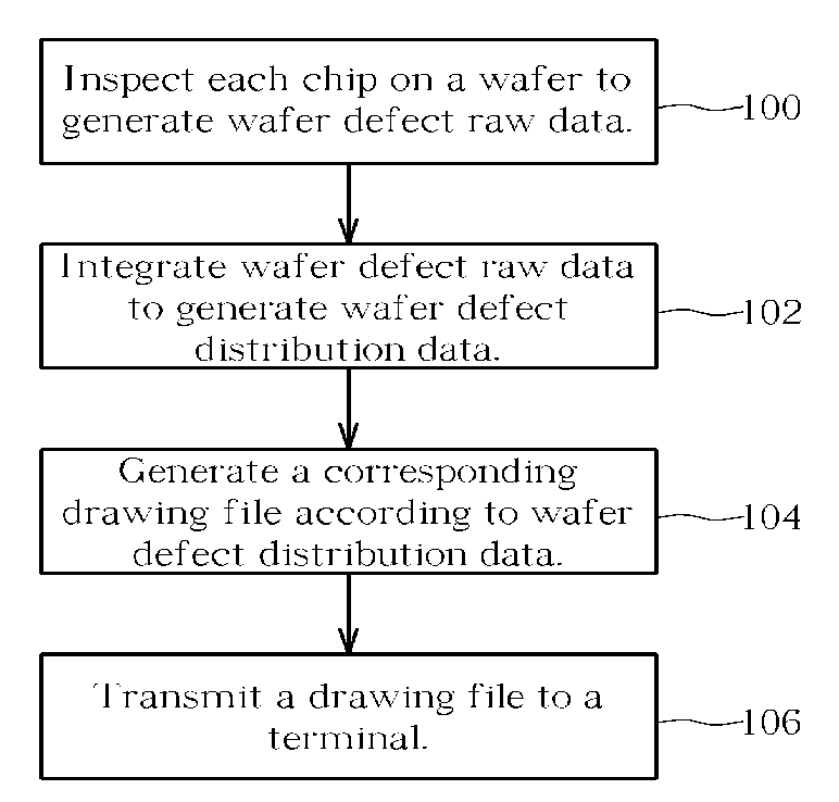
[0014]Please refer to FIG. 1. FIG. 1 is a flow chart of a method of managing wafer defects according to the present invention including:

[0015]Step 100: perform an inspection step to inspect defects on each chip on a wafer and generate corresponding wafer defect raw data;

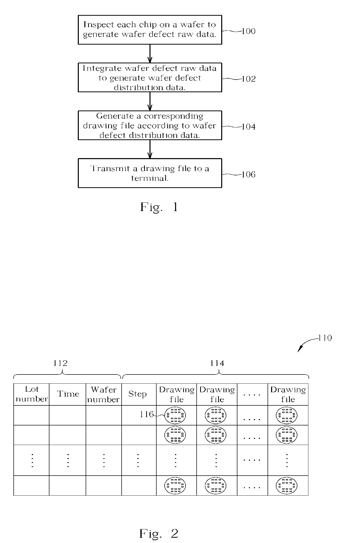
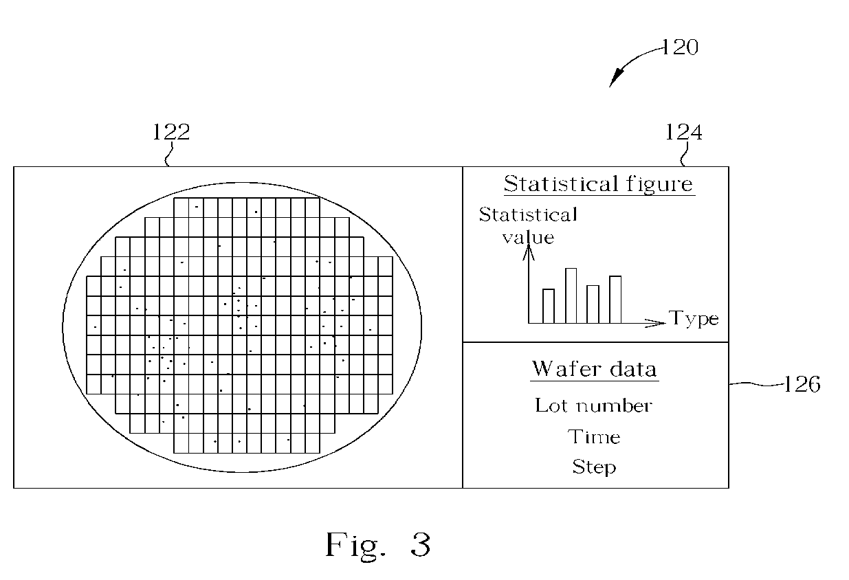
[0016]Step 102: perform a data pre-treatment step with a server to integrate the wafer defect raw data of each chip on the same wafer and generate wafer defect distribution data for recording distribution position, type, and size of defects relative to the whole wafer;

[0017]Step 104: perform a drawing pre-treatment step with the server to generate a corresponding drawing file according to defect distribution data of each wafer to display each distribution mode of defects on each wafer; and

[0018]Step 106: transmit the drawing file to a terminal with a server when the terminal engineer wants to view the wafer defect distribution such that these terminals do not need to receive the wafer defect raw data and terminal use...


PUM


Abstract

A method of managing wafer defects includes inspecting each chip in a wafer to generate a unit of wafer defect raw data, using a server to integrate the unit of wafer defect raw data to generate a unit of wafer defect distribution data for recording positions, types, and sizes of defects, using the server to generate a corresponding drawing file according to the unit wafer defect distribution data to show all kinds of defect distributions, and transmitting the drawing file to a terminal such that terminal users can view the defect distributions without receiving the unit of wafer defect raw data.

Description

BACKGROUND OF INVENTION[0001]1. Field of the Invention[0002]The invention relates to a method of managing wafer defects, and more particularly, to a method of managing wafer defects using a server to generate corresponding drawing files according to wafer defect raw data in advance for decreasing terminal calculations.[0003]2. Description of the Prior Art[0004]In the semiconductor manufacturing process, the semiconductor foundry performs defect inspection such as bright field or dark field defect inspection with wafers after a manufacturing process to improve wafer yield of the process. This kind of inspection is mostly performed on each chip on a wafer. In the inspection process, the inspection equipment takes an assigned position on a wafer as a standard position, and the inspection result of the standard position as a standard value to measure inspection results of another positions on the chip relative to the standard value and record them as the defect raw data. For integrating...

Claims


Application Information

Patent Timeline
Patent Type & Authority Patents(United States)
IPC IPC(8): G06K9/00
CPCG01N21/9501
Inventor TAI, HUNG-ENCHEN, CHIA-YUNWANG, SHENG-JEN
Owner POWERCHIP SEMICON MFG CORP
Why Eureka
Try Eureka