Memory-module board layout for use with memory chips of different data widths

a memory module and data width technology, applied in the field of memory modules, can solve problems such as increased inventory costs or delayed or lost sales

Active Publication Date: 2008-08-19
KINGSTON DIGITAL CO LTD
View PDF18 Cites 86 Cited by
  • Summary
  • Abstract
  • Description
  • Claims
  • Application Information

AI Technical Summary

Problems solved by technology

Predicting the exact product mix of ×4 and ×8 chip modules can be difficult, and incorrectly predicting the product mix may lead to increased inventory cost or delayed or lost sales.

Method used


Image

  • Memory-module board layout for use with memory chips of different data widths
  • Memory-module board layout for use with memory chips of different data widths
  • Memory-module board layout for use with memory chips of different data widths

Examples


Embodiment Construction

[0017]The present invention relates to an improvement in memory modules. The following description is presented to enable one of ordinary skill in the art to make and use the invention as provided in the context of a particular application and its requirements. Various modifications to the preferred embodiment will be apparent to those with skill in the art, and the general principles defined herein may be applied to other embodiments. Therefore, the present invention is not intended to be limited to the particular embodiments shown and described, but is to be accorded the widest scope consistent with the principles and novel features herein disclosed.

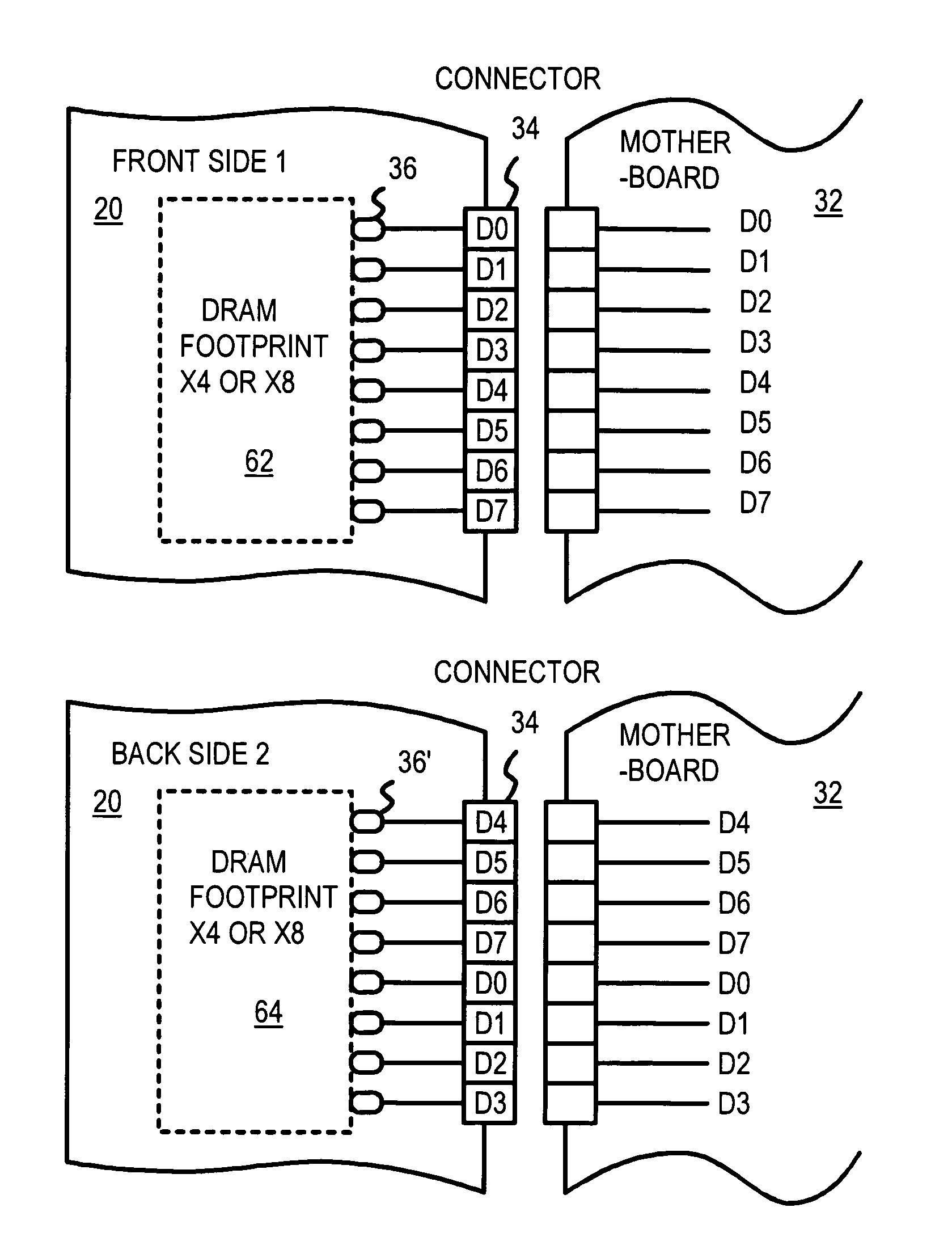
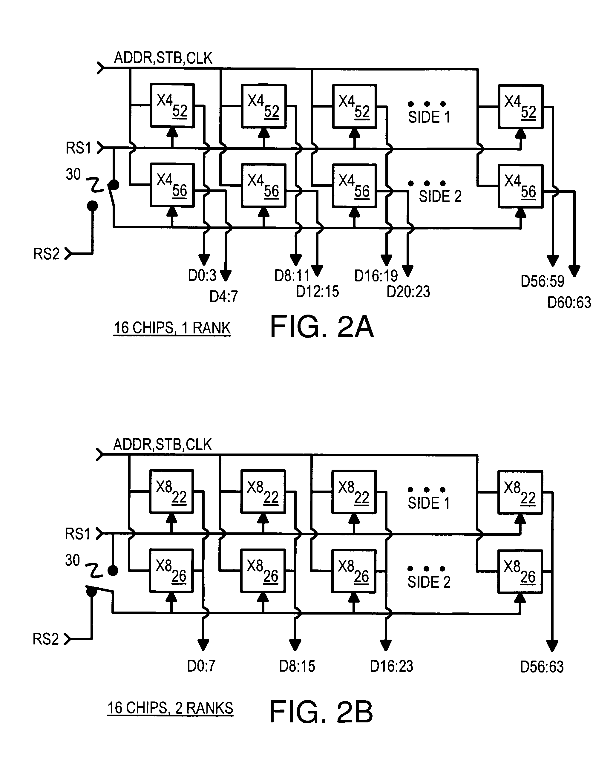
[0018]The inventors have discovered that a universal memory module printed-circuit board (PCB) layout may be used for different types of memory modules. In particular, a multi-type layout for a PCB can be used for building memory modules that use either ×4 or ×8 DRAM chips. A single footprint on the PCB layout can have either a ×4 or a...


PUM


Abstract

A memory module substrate printed-circuit board (PCB) has multi-type footprints and an edge connector for mating with a memory module socket on a motherboard. Two or more kinds of dynamic-random-access memory (DRAM) chips with different data I / O widths can be soldered to solder pads around the multi-type footprints. When ×4 DRAM chips with 4 data I / O pins are soldered over the multi-type footprints, the memory module has a rank-select signal that drives chip-select inputs to all DRAM chips. When ×8 DRAM chips with 8 data I / O pins are soldered over the multi-type footprints, the memory module has two rank-select signals. One rank-select drives chip-select inputs to front-side DRAM chips while the second rank-select drives chip-select inputs to back-side DRAM chips. Wiring traces on the PCB cross-over data nibbles between the solder pads and the connector to allow two ×4 chips to drive a byte driven by only one ×8 chip.

Description

FIELD OF THE INVENTION[0001]This invention relates to memory modules, and more particularly to board layouts of memory modules supporting memory chips of varying data widths.BACKGROUND OF THE INVENTION[0002]Many types of electronics systems contain memory. A common, low-cost memory is dynamic-random-access memory (DRAM). Rather than sell individual DRAM chips, such chips are often pre-assembled into modules that can be inserted into sockets in a wide variety of systems. Such memory modules have gained enormous popularity in recent years. Most personal computers (PC's) are shipped with sockets for memory modules so the PC user can later add additional modules, increasing the memory capacity of the PC. High-volume production and competition have driven module costs down dramatically, benefiting the PC buyer.[0003]Memory modules are made in many different sizes and capacities, such as older 30-pin and 72-pin single-inline memory modules (SIMMs) and newer 168-pin, 184-pin, and 240-pin d...

Claims


Application Information

Patent Timeline
Patent Type & Authority Patents(United States)
IPC IPC(8): H01L23/34G11C5/06H05K7/00
CPCG11C5/04G11C8/12H05K1/181G11C2029/1804H05K2201/09245H05K2201/09954H01L2924/0002H05K2201/10689H05K2203/1572H01L2924/00Y02P70/50
Inventor NGUYEN, HENRY H. D.BURLINGTON, MARK
Owner KINGSTON DIGITAL CO LTD
Why Eureka
Try Eureka