COB-typed LED package with phosphor

a technology of led packaging and tag phosphor, which is applied in the direction of electroluminescent light sources, chemistry apparatuses and processes, and compositions of light sources. it can solve the problems of difficult color temperature adjustment of white light generated through the yag phosphor, difficult high power of the packaging unit, and uncomfortable white generated ligh

Inactive Publication Date: 2008-09-23
LUSTROUS TECH
View PDF5 Cites 14 Cited by
  • Summary
  • Abstract
  • Description
  • Claims
  • Application Information

AI Technical Summary

Benefits of technology

[0010]Another objective of the present invention is to provide a LED package unit capable of generating comfortable white light.

Problems solved by technology

Comparatively, the LED package unit incorporating TAG phosphor is difficult to achieve high power because of the material property.
The LED package unit incorporating YAG phosphor is capable of generating light at high power, but the primary drawback is that the generated light often referred to a kind of “uncomfortable white”.
The white light generated through the YAG phosphor is hard to adjust its color temperature.
Not only uncomfortable to the human eyes, it is even not capable of passing some specific standards, such as the product safety standard of the medical field or the traffic safety field.

Method used


Image

  • COB-typed LED package with phosphor
  • COB-typed LED package with phosphor
  • COB-typed LED package with phosphor

Examples


Embodiment Construction

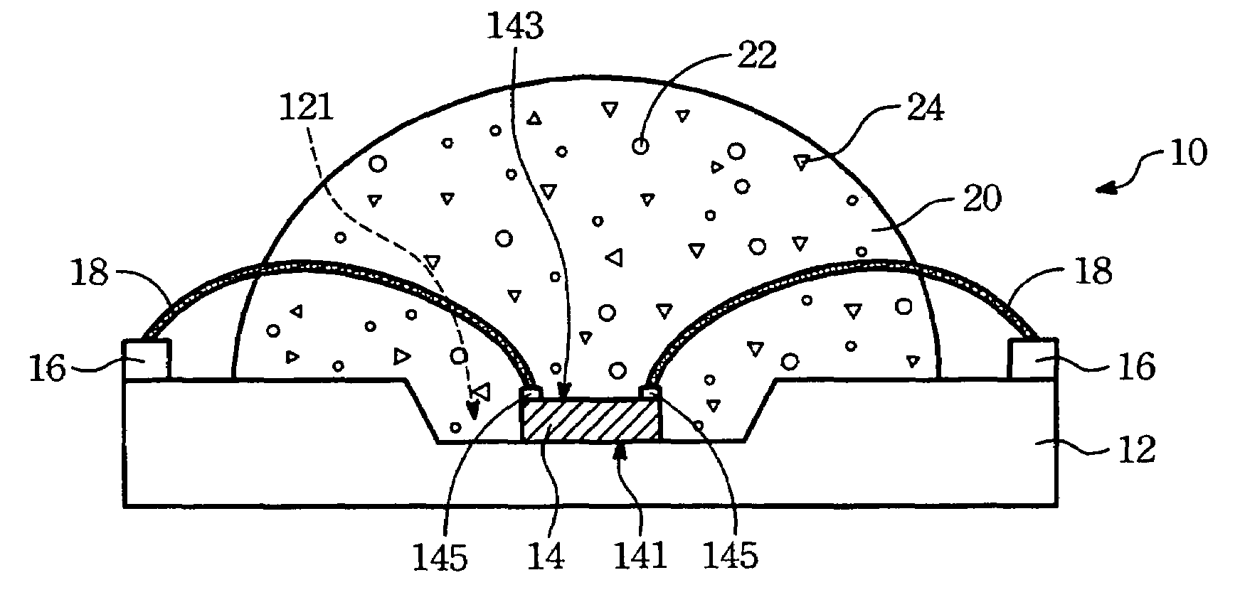
[0023]Please refer to FIG. 1. FIG. 1 shows a cross section view of the present LED package unit. The LED package unit comprising a substrate 12, a LED chip 14, at least two electrodes 16, at least two wires 18, a gel 20, a first wavelength-converting material 22 and a second wavelength-converting material 24. The substrate 12, such as a thin metal plate, has a concave 121 for containing the LED chip 14.

[0024]The LED chip 14, which is disposed in the concave 121, comprises a top-face 143, a bottom-face 141 for jointing with the substrate 12, and at least two chip-electrodes 145 disposed on the top-face 143. While conducted with electric current, the LED chip 14 emits light of a first wavelength.

[0025]The at least two electrodes 16 is disposed on the substrate 12, and preferably they are disposed in the margin area of one face of the substrate 12 that containing the LED chip 14. The at least two wires respectively connects one of the chip-electrode 145 with one of the electrode 16.

[00...


PUM


Abstract

A light emitting diode (LED) package unit, including a substrate having a concave, a LED chip, at least two electrodes, at least two wires, a gel and a first wavelength-converting material. The LED chip, disposed in the concave, including a top-face, a bottom-face for jointing with the substrate, and at least two chip-electrodes. The LED chip emits light of a first wavelength. The electrodes are disposed on the substrate. The wires are respectively connecting one of the chip-electrode with one of the electrode. The gel is disposed to seal the LED chip and the wires. The first wavelength-converting material including Sr—Si—O—N:Eu is doped within the gel. The first wavelength-converting material absorbs light of the first wavelength and emits light of a second wavelength longer than the first wavelength.

Description

BACKGROUND OF THE INVENTION[0001](1) Field of the Invention[0002]The invention relates generally to a package structure of a light emitting diode (LED) device, and particularly to a chip-on-board (COB)-typed LED package with specific phosphors.[0003](2) Description of the Prior Art[0004]LEDs are now widely used as illuminators, indicators or displays in many kinds of electronic products or industrial applications. One of the advantages of LEDs is that they consume much less electricity, or energy, as comparing with other traditional lighting devices. This is because that LEDs are known as solid state devices that generate light through a luminescence process. Thus the light generated by LEDs is referred to “cold light”. Besides, another advantage of LEDs is its small size. An LED are provided as a semiconductor chip. Hence, LEDs can meet the size-reducing requirement of modern electronic products, especially the delicate electronic products.[0005]LEDs based on the III-nitride materi...

Claims


Application Information

Patent Timeline
Patent Type & Authority Patents(United States)
IPC IPC(8): H01L29/22H01L23/02H01L33/00H01L31/12H01L27/15H01L29/24H01L31/0203H01L29/267H01L29/16H01L33/50H01L33/56H01L33/62
CPCC09K11/0883C09K11/7732C09K11/7734H05B33/14H01L33/501H01L33/502H01L33/56H01L2224/48091H01L33/62H01L2924/00014C09K11/77347
Inventor LIU, CHIA-CHICHENG, WEI-YUAN
Owner LUSTROUS TECH
Why Eureka
Try Eureka