Integral charge storage basement and wideband embedded decoupling structure for integrated circuit

a charge storage and integrated circuit technology, applied in the direction of fixed capacitor details, fixed capacitors, semiconductor/solid-state device details, etc., can solve the problems of increasing the complexity of electronic circuitry, the design of power distribution decoupling networks has become problematic, and the decoupling circuit has become increasingly complex, so as to reduce the number of bypass capacitors and eliminate the plethora of bypass capacitors. , the effect of saving component and assembly costs

Inactive Publication Date: 2008-09-23
GEOMAT INSIGHTS
View PDF14 Cites 47 Cited by
  • Summary
  • Abstract
  • Description
  • Claims
  • Application Information

AI Technical Summary

Benefits of technology

[0018]The present invention is a capacitive structure and technique for allowing near-instantaneous charge transport and reliable, wide-band RF ground paths in integrated circuit devices such as integrated circuit dies, integrated circuit packages, printed circuit boards, and electronic circuit substrates.
[0020]A lossy signal absorption ring structure is implemented, preferably at the capacitor's perimeter, to eliminate or greatly reduce the edge reflection and thereby eliminate or greatly reduce the resonances that determine the upper frequency limit of the capacitor's use. The perimeter loss function can be accomplished by any and all combination of the four absorptive modes: conductive loss, dielectric loss, magnetic loss, and radiative loss. Also, the perimeter loss function can be accomplished using a continuous or discontinuous ring of absorptive material. The lossy material can be patterned in discontinuous pieces. While in the preferred embodiment the lossy material is formed as a continuous ring, it in fact can be implemented as discrete lossy chunks scattered in a pattern to obtain the desired perimeter loss function. The idea is to absorb the laterally flowing waves without impeding the supply of charge to the components the device is designed to supply charge for, and any means of achieving the absorption is acceptable. This includes the following methods but does not preclude other methods: adding or taking away material, or converting the properties of materials so that they selectively become absorptive in a pattern that absorbs the laterally flowing waves while minimizing any restriction of the charge flow vertically out of or into the charge storage device. This pattern could be anywhere within the volume of the charge storage device and is not limited to the physical perimeter of a layer. What is shown in the detailed description and drawings as examples of this invention are just that. They are examples of patterned lossy material that dampen the laterally flowing waves that create resonances which limit the upper frequency usefulness of capacitors without interfering with charge transport to the external circuitry from and to these capacitors. Basically this pattern of lossy material is designed to inhibit the ebb and flow of the charge within the capacitor without interfering with the ability to move charge in and out of the capacitor. For this reason, the loss generally (but not always) appears at the physical perimeter of the CSB where the reflections take place. The invention includes all methods, and materials of obtain a loss pattern within a capacitor that inhibits the lateral flowing waves induced within a capacitor whenever charge is added or removed while minimizing the restriction of charge transport in and out of the capacitor itself. The exact loss pattern can also be tailored for specific applications and specific placement of parts. Additional isolation can be provided between individual circuits by implementing a respective signal absorption ring around each circuit that needs additional isolation
[0021]In implementation, an integrated circuit device includes an integral set of high-dielectric layers interleaved with highly-conductive layers, with at least one signal absorption ring implemented on or in at least one of the conductive and / or dielectric layers. The signal absorption ring operates to dampen lateral traveling waves generated in the structure so as to eliminate or at least substantially mitigate the resonant frequency limitations of the plate capacitor formed by the structure.
[0022]The structure of integral charge storage layers with signal absorption ring(s) (termed herein “charge storage basement” or “CSB”) provides near-instantaneous charge delivery and good wide-band RF shorts, that is high wide-band shunt admittance, at any point on the surface of any substrate containing a CSB. In the context of the present invention, a “good” RF short (1) is non-resonant (i.e. does not become inductive or open at certain frequencies), (2) has low RF impedance, and 3) the charge is stored physically and electrically close to the capacitor terminal where the charge is to be accessed. The availability of near-instantaneous charge delivery and good wide-band RF shorts anywhere on the substrate of the integrated circuit or chip package allows for the development of greatly simplified circuits with fewer parts and therefore greater robustness, lower manufacturing costs, and faster design time. The predictability of the CSB to provide wide-band (simultaneous high and low frequencies) shunt admittance anywhere on the IC's / PCB's / (any other substrate's) surface significantly contributes to electronic circuit development in a single prototype cycle, drastically reducing time-to-market.
[0024]In one preferred embodiment of the CSB of the invention, at least one of the conductive layers is connected to a power source and operates as a power plane, while at least one other of the conductive layers is connected to the circuit / chip / board ground and operates as a ground plane. The signal absorption ring(s) are preferably implemented at the outside edge of the layer(s) and / or circuitry to be isolated and surrounds the internal useful area of the power and / or ground layer(s) where charge storage and power supply decoupling takes place. Ideally the signal absorption ring(s) absorb all or most of the energy of any waves generated within the CSB, thereby eliminating or substantially mitigating the Nλ / 2 resonances that would otherwise limit the upper frequency of the buried capacitor.

Problems solved by technology

The design of power distribution decoupling networks has become problematic due to the ever-increasing complexity of electronic circuitry.
Over time these decoupling circuits have become increasingly complex and are projected to become more so as PCB, Integrated Circuit (IC), and other substrate circuitry increases in diversity and bandwidth.
The design of power distribution decoupling networks is fraught with problems and tradeoffs.
First, capacitors are not capable of bypassing both low and high frequencies.
The power distribution network consisting of these capacitors, resistors, and inductive line lengths, is therefore generally underdamped and prone to instabilities which compromise the performance and isolation of the various generally diverse circuits that they feed power to.
This traditional method of decoupling is power inefficient as well as costly in terms of manufacturing, reliability and board space.
Because DC current must travel through the series damping elements, this approach has the additional flaw of wasting power (I2R losses) in power-distribution circuits.
Furthermore, a multitude of capacitors must be purchased, inventoried, and handled, requiring labor and machine time to install them.
Once installed, the capacitors contribute to reducing the reliability of the whole assembly tremendously by introducing two solder connections per component (e.g., capacitors and dampening resistors).
One of the highest failure mechanisms in a modern surface mount board are stress failures at the solder joints themselves as well as the growing of metallic oxide dendrites between the component solder pads when biased circuit boards are subjected to humid or wet environments.
This problem may become worse with the advent of the new “Pb free” solders that manufacturers will be required to use by Jul. 1, 2006.
However, internal reflections off the finite boundaries of such a capacitor induce many resonances in its admittance, destroying the decoupling characteristics of the capacitor at its parallel-resonant frequencies, where its admittance is relatively small.
Whereas using several layers of a circuit board to create a whole board integral capacitor provides charge physically close to the components requiring charge, it does not solve the fundamental resonance problems that limit the upper frequency use of the capacitor.
So, once again, while converting several of the board's layers to one large integral capacitor solves the problem of the stored charge being physically far from circuits requiring the charge, it does not address the fundamental self resonance problems that result from attempting to use a single large capacitor physically big enough to be close to all board components and electrically large enough to bypass the lowest frequencies of the wide band circuitry.
The circuit isolation fails at these points, frequently resulting in unacceptable levels of crosstalk and circuit instabilities due to unintended feedback.

Method used


Image

  • Integral charge storage basement and wideband embedded decoupling structure for integrated circuit
  • Integral charge storage basement and wideband embedded decoupling structure for integrated circuit
  • Integral charge storage basement and wideband embedded decoupling structure for integrated circuit

Examples


Embodiment Construction

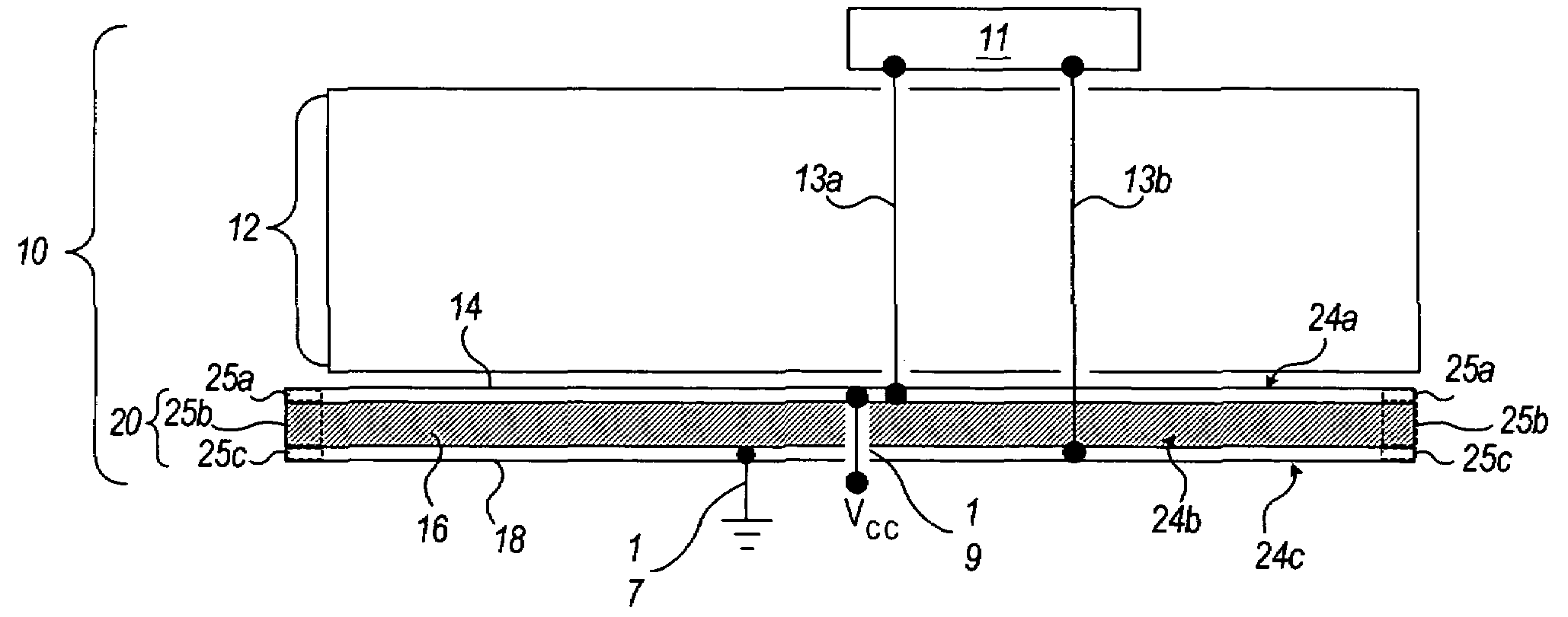
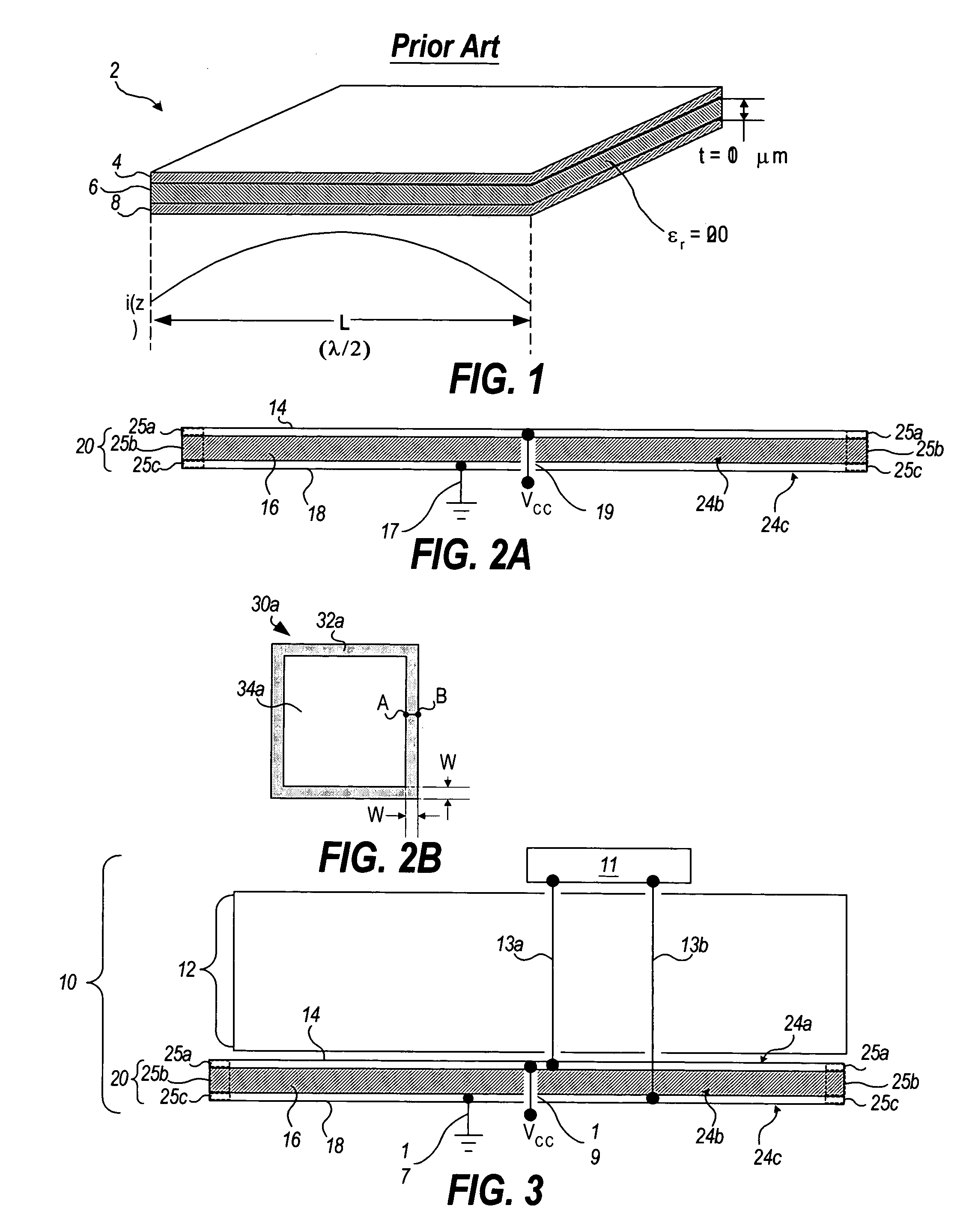
[0059]In order to more fully understand the present invention, we turn now to consider the prior art parallel plate capacitor structure 2 diagrammed in FIG. 1. The structure 2 is formed with a dielectric 6 sandwiched between two conductive plates 4 and 8 at different voltage potentials (e.g., VCC and ground, respectively). The structure 2 exhibits resonances due to waves that move laterally in the capacitor and that are reinforced by multiple reflections off the edges of the capacitor at frequencies where the path length (L) is a multiple (N) of a half (½) of a wavelength, λ—that is, L=Nλ / 2. The first resonance, f1, occurs at the frequency where the capacitor is half a wavelength (λ / 2) long. Additional resonances occur whenever the length is an integer (N) multiple of λ / 2, giving the frequency of the Nth resonance, fN, as

[0060]fN=N2⁢cL⁢ɛr(1)

[0061]where εr is the relative dielectric constant of the material of the dielectric 6 separating the plates 2 and 4 of the capacitor and c is t...


PUM


Abstract

A capacitive structure and technique for allowing near-instantaneous charge transport and reliable, wide-band RF ground paths in integrated circuit devices such as integrated circuit dies, integrated circuit packages, printed circuit boards, and electronic circuit substrates is presented. Methods for introducing resistive loss, dielectric loss, magnetic loss, and / or radiation loss in a signal absorption ring implemented around a non-absorptive area of one or more conductive layers of an integrated circuit structure to dampen laterally flowing Electro-Magnetic (EM) waves between electrically adjacent conductive layers of the device are also presented.

Description

BACKGROUND OF THE INVENTION[0001]The design of power distribution decoupling networks has become problematic due to the ever-increasing complexity of electronic circuitry. Power supply distribution on a typical Printed Circuit Board (PCB) is accomplished with an elaborate decoupling network consisting of a multitude of shunt capacitors and series dampening elements. A major concern in modern PCB design is power supply isolation between the various circuits on the PCB. To that end, complex decoupling networks have evolved to minimize direct coupling and Electro-Magnetic-Interference (EMI) between these circuits along the power supply distribution lines. These circuits consist of various bypass capacitors that collectively provide high shunt admittance across all frequencies on the PCB, and series dampening devices which are generally resistors and ferrite beads. Over time these decoupling circuits have become increasingly complex and are projected to become more so as PCB, Integrated...

Claims


Application Information

Patent Timeline
Patent Type & Authority Patents(United States)
IPC IPC(8): H01G4/228
CPCH01G4/33H01L23/642H05K1/0234H05K1/0233H01L23/50H01L23/66H01L2924/3011H05K1/0225H01L2224/16H05K1/167H05K2201/086H05K2201/093H05K2201/09309H05K2201/09663
Inventor BARNETT, RONALD J.
Owner GEOMAT INSIGHTS
Why Eureka
Try Eureka