Gate driving circuit

a driving circuit and gate technology, applied in logic circuits, oscillator generators, pulse techniques, etc., can solve problems such as current instability, gate driving circuit b>10/b> is usually harmful to the output load device, and unstable driving curren

Inactive Publication Date: 2008-10-07
ETRON TECH INC
View PDF2 Cites 6 Cited by
  • Summary
  • Abstract
  • Description
  • Claims
  • Application Information

AI Technical Summary

Benefits of technology

[0011]It is a secondary object of the present invention to provide a gate driving circuit which keeps the voltage source-to-gate of the PMOS transistor a constant in the ON state, so that a constant current is providing for the output load device.
[0012]It is another object of the present invention to provide a gate driving circuit, further comprising a pull down circuit for quickly pulling the gate voltage down to the target value of the voltage following bias circuit.

Problems solved by technology

The conventional gate driving circuit 10 of the prior art has a drawback of causing an unstable driving current if the external supply voltage VDD varies or has a voltage drift.
The current instability caused by the conventional gate driving circuit 10 is usually harmful for the output load device 19 and other load devices.
It may drive the load devices to the unstable state or cause damages to the load devices.

Method used


Image

  • Gate driving circuit
  • Gate driving circuit
  • Gate driving circuit

Examples


Embodiment Construction

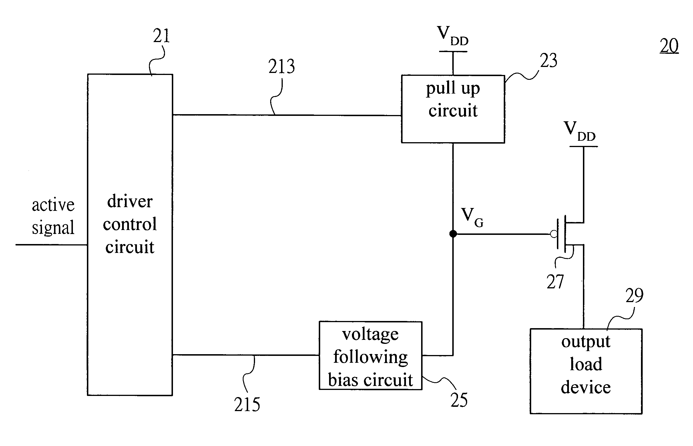
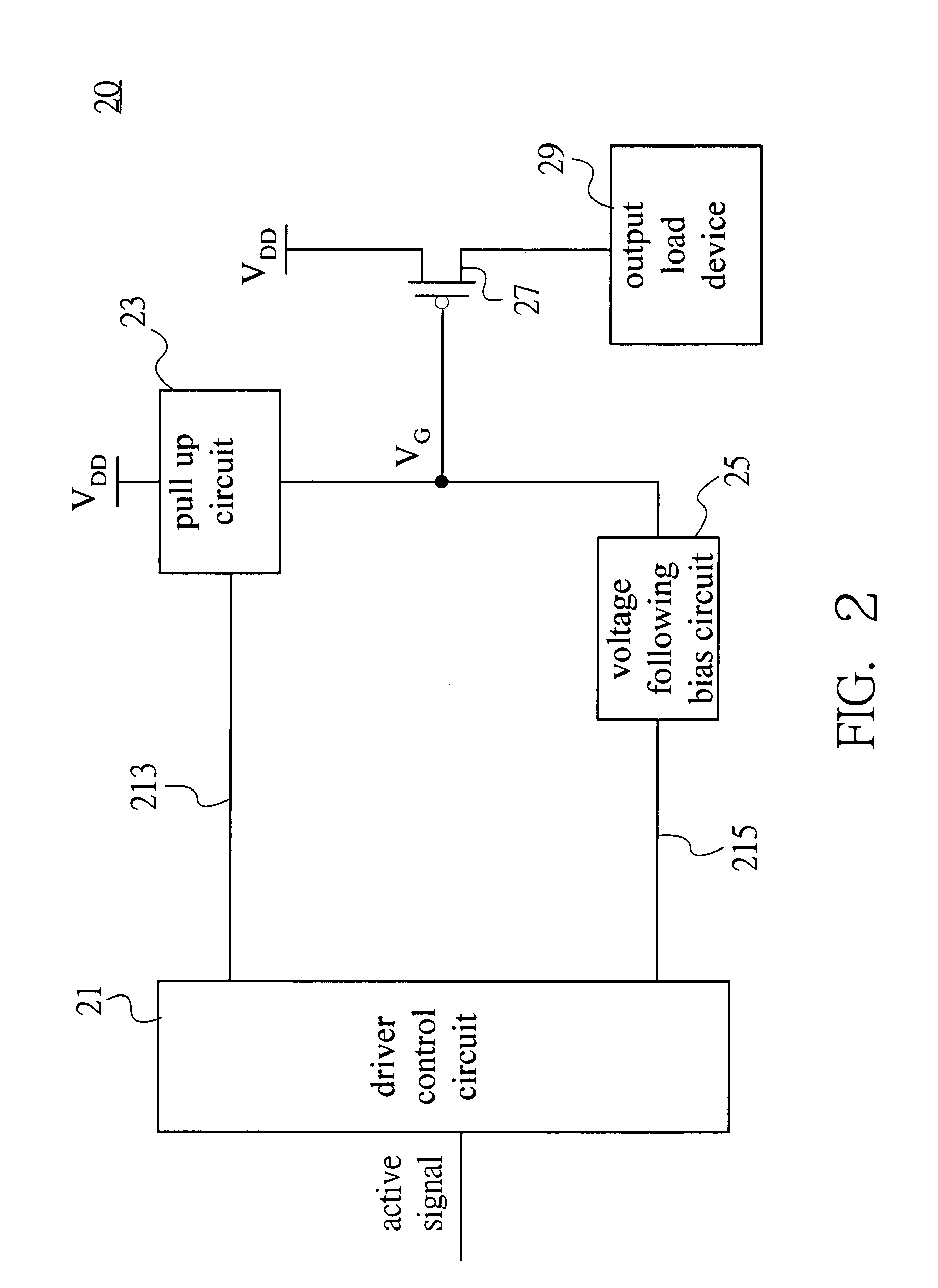
[0020]Referring to FIG. 2, there is shown a block diagram of a preferred embodiment of the present invention. As shown in the figure, the gate driving circuit 20 comprises a driver control circuit 21, a pull up circuit 23, a voltage following bias circuit 25, and a MOS transistor 27.

[0021]The pull up circuit 23 is connected to the driver control circuit 21 through the first signal line 213. The voltage following bias circuit 25 is connected to the driver control circuit 21 through the second signal line 215. The pull up circuit 23 and the voltage following bias circuit 25 are both connected to the gate of the MOS transistor 27 for driving the MOS transistor 27 to the ON state or the OFF state.

[0022]In the present embodiment, the MOS transistor 27 is a PMOS transistor with the source connected to the external supply voltage VDD and the drain connected to the output load device 29.

[0023]The driver control circuit 21 generates a pull up signal or a pull down signal according to an acti...


PUM


Abstract

The present invention relates to a gate driving circuit, comprising a driver control circuit, a voltage following bias circuit, a pull up circuit and a MOS transistor. The driver control circuit receives an active signal and generates a pull up signal or a pull down signal. In case of the pull up signal, the MOS transistor is turned to the OFF state by the pull up circuit, and there is no current for the output load device. In case of the pull down signal, the MOS transistor is turned to the ON state by the voltage following bias circuit. The driving voltage for the gate of the MOS transistor has a constant voltage drop according to the external supply voltage. Therefore, the gate driving circuit of the present invention provides a constant current for the output load device.

Description

FIELD OF THE INVENTION[0001]The present invention relates to a gate driving circuit, more particularly to a gate driving circuit that can provide a constant current for the output load device.BACKGROUND OF THE INVENTION[0002]In general, there would be a current source control device between the current source and an output load device. The current source control device, such as a MOS transistor, always needs a gate driving circuit for providing driving voltages to control the ON / OFF state of the current source control device. The current source control device provides a driving current for the output load device when it is in the ON state.[0003]Referring to FIG. 1, there is shown a circuit diagram of a conventional gate driving circuit of the prior art. As shown in the figure, the gate driving circuit 10 comprises a driver control circuit 11, a pull up circuit 13, a pull down circuit 15 and a PMOS transistor 17.[0004]When the driver control circuit 11 receives an active signal, it g...

Claims


Application Information

Patent Timeline
Patent Type & Authority Patents(United States)
IPC IPC(8): H03B1/00
CPCH03K17/145
Inventor LIU, YAO YICHANG, YEN-AN
Owner ETRON TECH INC
Why Eureka
Try Eureka