Method of producing multilayer interconnection board

a multi-layer interconnection and interconnection board technology, applied in the direction of resistive material coating, metallic material coating process, pretreatment surface, etc., can solve the problem that the obtained via hole ends up being larger than the desired siz

Inactive Publication Date: 2008-10-21
SHINKO ELECTRIC IND CO LTD
View PDF3 Cites 4 Cited by
  • Summary
  • Abstract
  • Description
  • Claims
  • Application Information

AI Technical Summary

Benefits of technology

[0023]A specific object of the present invention is to provide a method of producing a multilayer interconnection board that is able to reduce residual resin at the bottom of a via hole and prevent broadening of the via hole when removing the residual resin.
[0029]According to the present invention, by using a thermal setting resin member having a thermal setting temperature higher than that of the resin member as the residual resin removing member, the resin member may be processed by imprinting press at a temperature lower than the temperature at which the thermal setting resin member cures completely, and an un-cured portion of the thermal setting resin member having higher solubility may be dissolved after imprinting press, hence, the residual resin member can be removed in a shorter time than in the related art.
[0031]According to the present invention, the residual resin removing member can be selectively dissolved, and this prevents the resin member from being dissolved.
[0033]According to the present invention, a conductive resin is provided on a via connecting portion of an interconnection layer connected with a via, and when forming a via hole by imprinting press; the amount of the residual resin member on the conductive resin is smaller than in the related art, thus, the residual resin member can be removed in a shorter time than in the related art.

Problems solved by technology

Even when forming the via hole by a laser, because the same step is carried out of removing the residual resin by using the resin solvent, the same problem arises in that the obtained via hole ends up being larger than a desired size.

Method used


Image

  • Method of producing multilayer interconnection board
  • Method of producing multilayer interconnection board
  • Method of producing multilayer interconnection board

Examples


first embodiment

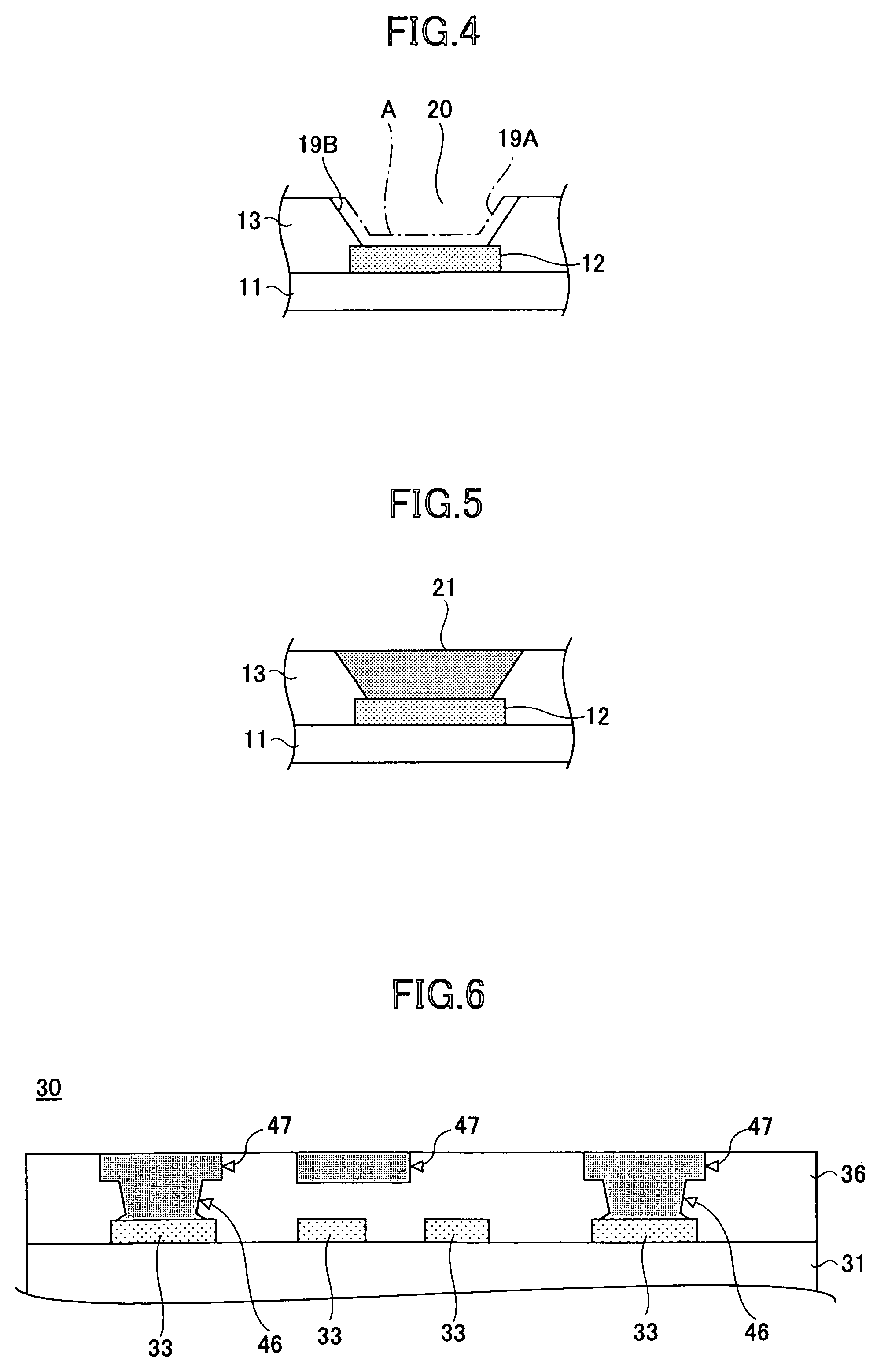
[0064]FIG. 6 is a cross-sectional view of a multilayer interconnection board 30 according to a first embodiment of the present invention.

[0065]As illustrated in FIG. 6, the multilayer interconnection board 30 is a build-up board with multilayer interconnection structures formed on two sides of a substrate 31 (also referred to as a core substrate). The multilayer interconnection board 30 includes the substrate 31, interconnections 33, 47 formed on the surface of the substrate 31, a via 46, and resin 36.

[0066]The interconnection 33 is formed on the substrate 31. On the substrate 31 with the interconnection 33 formed thereon, the resin 36 is formed. In the resin 36, the via 46 and the interconnection 47 are formed.

[0067]The via 46 is formed on a via-connecting portion of the interconnection 33. Here, “a via-connecting portion” is a portion of the interconnection 33 to which the via 46 is connected. The via 46 is formed by filling metal into a via hole 44 (refer to FIG. 12). The via 46 ...

second embodiment

[0090]FIG. 14 is a cross-sectional view of a multilayer interconnection board 30 according to a second embodiment of the present invention.

[0091]In FIG. 14 and the subsequent drawings, the same references are used for the same elements as those shown in the first embodiment and the overlapping descriptions are omitted.

[0092]As illustrated in FIG. 14, the interconnection 33 is formed on the substrate 31. In FIG. 14, a via-connecting portion 33A of the interconnection 33 is indicated.

[0093]FIG. 15, continuing from FIG. 14, is a cross-sectional view showing a step of the method of forming the multilayer interconnection board 30 according to the present embodiment of the present invention.

[0094]As illustrated in FIG. 15, a photosensitive resist 50 is deposited on the via-connecting portion 33A of the interconnection 33.

[0095]The photosensitive resist 50 may be formed by printing, ink jetting, or other well-known methods. If the photosensitive resist 50 is a positive type, the photosensi...

third embodiment

[0109]FIG. 21 is a cross-sectional view of a multilayer interconnection board 60 according to a third embodiment of the present invention.

[0110]In FIG. 21 and the subsequent drawings, the same references are used for the same elements as those shown in the previous embodiments and the overlapping descriptions are omitted.

[0111]As illustrated in FIG. 21, the multilayer interconnection board 60 is a built-up board with multilayer interconnection structures formed on two sides of a substrate 31. The multilayer interconnection board 60 is characterized in that a conductive resin 55 is interposed between the interconnections 33 and a via 52.

[0112]Specifically, the multilayer interconnection board 60 includes the substrate 31, interconnections 33, 47 formed on the substrate 31, a via 52, resin 36, and conductive resin 55.

[0113]The interconnection 33 is formed on the substrate 31. The conductive resin 55 is formed in the via-connecting portion 33A of the interconnection 33 (refer to FIG. 2...


PUM

PropertyMeasurementUnit
photosensitiveaaaaaaaaaa
temperatureaaaaaaaaaa
solubilityaaaaaaaaaa

Abstract

A method of producing a multilayer interconnection board is disclosed that includes the steps of processing a resin member on an interconnection layer by imprinting press, and removing residue of the resin member at the bottom of a via hole after forming the via hole. In the method of producing a multilayer interconnection board, a thermal setting resin, which has a setting temperature higher than that of the resin member, is applied on a via-connecting portion of the interconnection layer, the resin member is formed on the interconnection layer, an interconnection groove and a via hole are formed by imprinting press on the resin member by using a tool, and an un-cured portion of the high temperature setting resin is dissolved and removed by using a resin solvent. Thereby, residue of the resin member on the thermal setting resin is removed.

Description

BACKGROUND OF THE INVENTION[0001]1. Field of the Invention[0002]The present invention relates to a method of producing a multilayer interconnection board, and particularly, to a method of producing a multilayer interconnection board including the steps of processing a resin member on an interconnection by imprinting press, and removing residue of the resin member at the bottom of a via hole after forming the via hole.[0003]2. Description of the Related Art[0004]Along with requirements of enhanced performance and decreased size of recent electronic communication apparatuses, development has been made in the field of printed circuit boards, specifically, a multilayer interconnection board on which plural layers of interconnection circuits are stacked to increase density of the circuits. For example, there is a kind of multilayer interconnection board produced by a so-called “built-up method”, in which interconnection layers and insulating layers are stacked alternately, and vias are p...

Claims


Application Information

Patent Timeline
Patent Type & Authority Patents(United States)
IPC IPC(8): B05D5/12B05D3/00H05K3/46H05K3/00H05K3/10
CPCH05K3/005H05K3/107H05K3/4644H05K2203/308H05K2203/0108H05K2203/0582H05K2203/1189H05K3/465C02F3/1263C02F3/14C02F1/283
Inventor MURAMATSU, SHIGETSUGUYAMAZAKI, KATSUMI
Owner SHINKO ELECTRIC IND CO LTD
Why Eureka
Try Eureka