
Method and system for analyzing transaction level simulation data of an integrated circuit design

Active Publication Date: 2008-10-21
CADENCE DESIGN SYST INC
View PDF9 Cites 3 Cited by
  • Summary
  • Abstract
  • Description
  • Claims
  • Application Information

AI Technical Summary

Benefits of technology

[0002]Integrated circuit designers use many different techniques to verify the functional correctness of a design before chips are actually produced. One common method of verification is the use of simulation. Simulation dynamically verifies a design by monitoring behaviors of the design with respect to simulation test benches. Designers can simulate their designs at the signal level or at the transaction level. Simulating at the transaction level allows designers to debug their designs at a higher level of abstraction than when simulating at the signal level. Designers write software code which records the high-level functionality of their chip as a string of transaction blocks called a “fiber.” For example, a transaction block can be defined to represent a value “read” operation. In this way, designers can monitor transaction blocks rather than individual signals when debugging their designs.
[0004]A method of analyzing transaction level simulation data is to plot transaction fibers as a function of time. This method allows designers to better visualize the simulation data. In previous design verification tools, to view the number and position of child transaction blocks, a parent fiber had to be in an expanded state, i.e., child fibers of the parent fiber had to be plotted beneath the parent fiber. However, if all of the child fibers are visible, other fibers that a designer wishes to view may not be visible. Hence, there is a need for a method of analyzing transaction level simulation data such that designers will be able to determine if a fiber has any child fibers but at the same time be able to view several unrelated fibers.

Problems solved by technology

However, if all of the child fibers are visible, other fibers that a designer wishes to view may not be visible.

Method used


Image

  • Method and system for analyzing transaction level simulation data of an integrated circuit design
  • Method and system for analyzing transaction level simulation data of an integrated circuit design
  • Method and system for analyzing transaction level simulation data of an integrated circuit design

Examples


Embodiment Construction

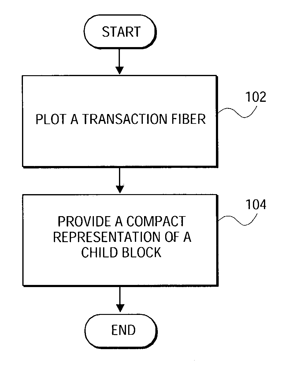
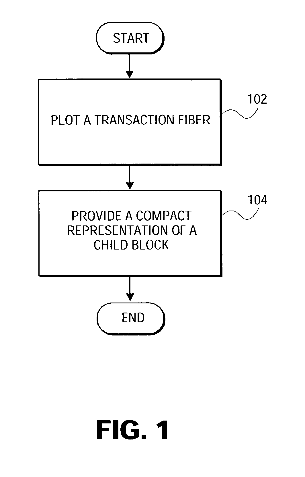
[0014]The present invention provides a method and system for analyzing transaction level simulation data of an integrated circuit design. FIG. 1 depicts a process flow diagram of an embodiment of the invention. In this embodiment, a transaction fiber is plotted (102). The transaction fiber comprises a transaction block. A compact representation of a child block of the transaction block is provided when the transaction fiber is in a collapsed state (104).

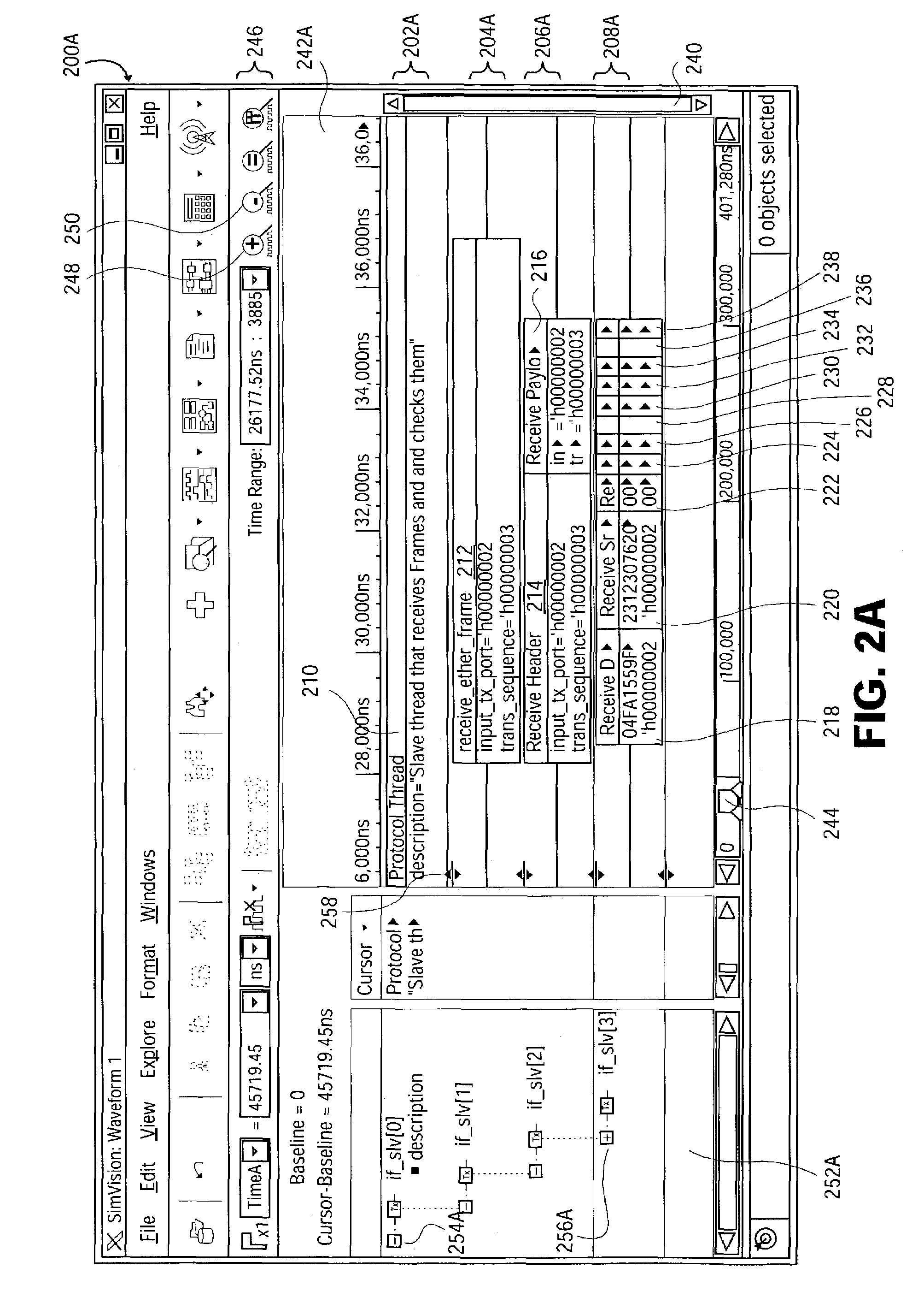
[0015]FIG. 2A shows a waveform window 200A in a simulation analysis tool displaying several transaction fibers in an expanded state in waveform area 242A according to an embodiment of the invention. In the embodiment, a minus sign on a button next to a fiber name signifies that the fiber is in an expanded state. For example, fiber if slv[0]202A, with a transaction block labeled “Protocol Thread”210, is in an expanded state as there is a minus sign on button 254A in signal list area 252A. Fiber 202A can be collapsed by clicking on but...


PUM


Abstract

A method and system for analyzing transaction level simulation data of an integrated circuit design. In an embodiment, a transaction fiber is plotted. The transaction fiber comprises a transaction block. A compact representation of a child block of the transaction block is provided when the transaction fiber is in a collapsed state. In one embodiment, the compact representation of the child block is provided by drawing a line segment below the transaction fiber.

Description

BACKGROUND AND SUMMARY[0001]The present invention is related to design verification tools. More particularly, the present invention is directed to a method and system for analyzing transaction level simulation data of an integrated circuit design.[0002]Integrated circuit designers use many different techniques to verify the functional correctness of a design before chips are actually produced. One common method of verification is the use of simulation. Simulation dynamically verifies a design by monitoring behaviors of the design with respect to simulation test benches. Designers can simulate their designs at the signal level or at the transaction level. Simulating at the transaction level allows designers to debug their designs at a higher level of abstraction than when simulating at the signal level. Designers write software code which records the high-level functionality of their chip as a string of transaction blocks called a “fiber.” For example, a transaction block can be defi...

Claims


Application Information

Patent Timeline
IPC IPC(8): G06F17/50
CPCG06F17/5022G06F30/33
Inventor MCLENNAN, MICHAEL J.
Owner CADENCE DESIGN SYST INC
Learn More