Polymer for sealing porous materials during chip production

a technology of porous materials and polymers, which is applied in the direction of other chemical processes, semiconductor/solid-state device details, chemistry apparatus and processes, etc., can solve the problems of introducing materials with intrinsic porosity, adverse effects or even destruction of the actual function of interlayer dielectrics (ilds), and exposed to contaminating chemical substances without any protection, etc., to reduce the dimensions of the recess

Active Publication Date: 2008-10-28
INFINEON TECH AG
View PDF18 Cites 6 Cited by
  • Summary
  • Abstract
  • Description
  • Claims
  • Application Information

AI Technical Summary

Benefits of technology

[0078]In the 150 nm technology generation which is currently in use, the metal track width is 150 nm, the ILD width is 150 nm, the metal track height is approx. 180-300 nm. The layer thickness of the polymer according to the invention is if possible 5 nm or below. For future technology generations, the metal / ILD widths and heights will become narrower. The 45 nm technology generation requires metal track / ILD widths of 45 nm. If an interlayer (liner, barrier layer) (e.g. 10 nm of TAN) is applied as well as a monolayer of polymer, there is no longer much space for a copper track. One advantage of the present invention is that the polymer compounds according to the invention can be applied in very low layer thicknesses.
[0079]A further advantage is that on account of the coating according to the invention it is even possible to do away with further lining of the inner walls prior to filling with copper.
[0080]The polymer compound can be applied as such or dissolved in a suitable solvent to the region to be treated, by means of spin-on methods or by dip coating.
[0081]The application is followed, in a preferred embodiment, by a heating step to dry the applied layer and / or to remove solvents and / or volatile constituents, in particular if the compound is applied together with a solvent.
[0082]In one preferred embodiment, an etching step is carried out after the application of the polymer compound and if appropriate the heating step, in order to remove excess polymer compound from the recess. In a particularly preferred embodiment, this can be directly followed by filling with copper. This offers the option of significantly reducing the dimensions of the recess compared to conventional methods, in which the inner walls are first lined with a barrier layer, and this allows further miniaturization.
[0083]Alternatively, in an embodiment which is likewise preferred, it is possible to line the inner wall using conventional methods, but with the layer thickness of the barrier layer in this case preferably being significantly less than has hitherto been customary. This can be achieved by prior coating with the polymers according to the invention and is likewise of benefit to miniaturization.

Problems solved by technology

In particular at the inner wall regions of the recesses etched into these materials, surface-exposed pores, and therefore pores which are connected by passages, are exposed to contaminating chemical substances without any protection.
In the context of chip production, the materials with a low dielectric constant then come into contact with various materials, for example water, atmospheric humidity or other chemicals, and these substances can penetrate into the cavities, thereby having an adverse effect or even destroying the actual function of the interlayer dielectrics (ILDs).
A drawback of this method, in the case of deposition of materials with a low dielectric constant, is that once again materials with an intrinsic porosity are introduced.
Moreover, the additional deposition narrows the recess, and consequently the recesses have to be made wider from the outset, which runs contrary to the aim of miniaturization for future technology generations.
A further drawback is that on account of the conformal deposition required, once again it is only possible to use CVD-type processes, which makes the chip production process more complicated and also runs the risk of the precursor compounds of this CVD material being able to penetrate into the pores.

Method used


Image

  • Polymer for sealing porous materials during chip production
  • Polymer for sealing porous materials during chip production
  • Polymer for sealing porous materials during chip production

Examples


example 1

[0118]Patterned wafers, i.e. wafers with uncovered walls of a low-k dielectric (carbon-doped silicon) were immersed for 1 h in a 10% by weight solution of the polymer according to the invention in cyclohexane. Alternatively, the solution can also be applied by spin-on methods. Group A used to produce the polymer was in each case methylene dimethylmethoxysilane, i.e. group A was introduced into the polymer chain, by way of example, via the compound (chloromethyl)dimethylmethoxysilane, with the result that group A was linked to the main polymer chain by a methylene group. The following radicals were respectively used as group B, with R3 for linking to the polymer main chain in each case being a methylene group.

[0119]

[0120]If group B was a benzotriazole radical, R1 was a methyl group at the ortho position with respect to the carbon atom which is linked to the N—R3 group. The polymer main chain used was polypropylene.

[0121]Groups A and B were present in approximately equal ratios in the...

example 2

[0126]The above method was repeated up to and including the removal of the solvent in the furnace.

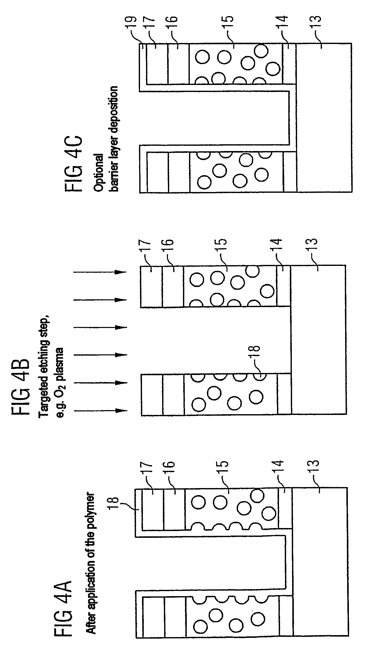
[0127]Then, a non-metallic thin SiC layer (a so-called liner layer with a thickness of 5 nm) was applied to the polymer monolayer deposited in this way by means of ALCVD or PVD.

[0128]The base of the recesses was etched clear by means of a short, targeted etching step (CF4 / H2 etching plasma). The polymer layer and the liner layer were retained at the side walls.

[0129]Then, a thin Ta layer with a thickness of 5 nm was applied by means of a PVD process as a metallic barrier layer.

[0130]As in Example 1, electrical evaluation of the fully processed wafers in each case resulted in excellent properties of the wafers produced in this way, i.e. it was not possible to determine any deterioration in the interlayer dielectric properties. Only in the case of the compounds with a benzotriazole radical as group B were occasional defects recorded once again.

[0131]Corresponding results were also obtaine...

example 3

[0132]Furthermore, to determine the porosities, the abovementioned compounds were applied to an Si wafer coated with a porous low-k material so as to coat the wafer with the polymer compounds over the entire surface. Ellipsometric porosity measurements using toluene in each case showed that the applied layers had no porosity. Only in the case of the benzotriazole derivates was a slight porosity determined from time to time.


PUM

PropertyMeasurementUnit
molecular weightaaaaaaaaaa
temperaturesaaaaaaaaaa

Abstract

A compound and method for sealing or protecting porous materials used in semiconductor fabrication, and in particular for protecting the inner walls of trenches or recesses or vias which are present in such materials. Specifically, compounds and the method of use of the compounds in which polymer compounds comprising functional groups A and B are used to seal surface-exposed pores in porous materials used in chip production.

Description

RELATED APPLICATIONS[0001]This application is a continuation of PCT patent application number PCT1 / EP2003 / 006527, filed Jun. 20, 2003, which claims priority to German patent application number 10227663.3, filed Jun. 20, 2002, the disclosures of each of which are incorporated herein by reference in their entirety.TECHNICAL FIELD[0002]The present invention relates to a method in which polymer compounds comprising functional groups A and B are used to seal surface-exposed pores in porous materials used in chip production, to the compounds for this purpose and to the use of the polymer compounds.BACKGROUND ART[0003]The integration of multiple metallizations in integrated circuits or chips requires major changes in terms of the material and technological processes in order to reduce delays, capacitances and couplings between different metal tracks. The replacement of silicon dioxide with dielectrics with a low dielectric constant (known as low-k materials or interlayer dielectrics—ILD) i...

Claims


Application Information

Patent Timeline
Patent Type & Authority Patents(United States)
IPC IPC(8): C08G77/28C08G77/26C09J143/04H01L21/312H01L21/768H01L23/532
CPCC09J143/04H01L21/3105H01L21/76831H01L21/76843H01L21/76844H01L23/5329H01L23/53295H01L21/02126H01L21/02203H01L2924/0002H01L23/53238H01L2924/00
Inventor HEILIGER, LUDGERSCHMIDT, MICHAELTEMPEL, GEORG
Owner INFINEON TECH AG
Why Eureka
Try Eureka