Perpendicular magnetic tunnel junction (pMTJ) devices employing a thin pinned layer stack and providing a transitioning start to a body-centered cubic (BCC) crystalline / amorphous structure below an upper anti-parallel (AP) layer

a technology of perpendicular magnetic tunnel junction and pinned layer stack, which is applied in solid-state devices, instruments, galvano-magnetic material selection, etc., can solve the problems of difficult integration of mtj stack structure into metal-oxide (mos) devices, as well as the etch process to form such mos devices, and achieve high tunnel magnetoresistance ratio (tmr), reduce pinned layer thickness, and prevent magnetic field bias

Active Publication Date: 2017-03-07
QUALCOMM INC
View PDF27 Cites 15 Cited by
  • Summary
  • Abstract
  • Description
  • Claims
  • Application Information

AI Technical Summary

Benefits of technology

[0015]Aspects of the present disclosure involve perpendicular magnetic tunnel junction (pMTJ) devices employing a thin pinned layer stack with a thin upper anti-parallel (AP) layer (AP2 layer). Another aspect of the present disclosure involves employing a combination of materials in the pMTJ device for a bottom anti-parallel (AP) layer (AP1 layer) and an anti-ferromagnetic coupling (AFC) layer in the thin pinned layer stack providing a transitioning start to a body-centered cubic (BCC) crystalline/amorphous structure below an upper AP layer (AP2 layer). This can promote a high tunnel magnetoresistance ratio (TMR) with reduced pinned layer thickness as an example. In this regard, in exemplary aspects disclosed herein, a pMTJ is provided that includes an MTJ stack structure. The MTJ stack structure includes a free layer and a pinned layer disposed on sides of a tunnel barrier layer having a body-centered cubic (BCC) crystalline/amorphous structure (e.g., a Magnesium Oxide (MgO) layer) to provide TMR. To reduce or prevent magnetic field bias of the pinned layer on the free layer, the pinned layer includes a synthetic anti-ferromagnetic (SAF) structure that includes a first anti-parallel (...

Problems solved by technology

Increased AP1 layer and AP2 layer thicknesses also makes integration of the MTJ stack structure ...

Method used


Image

  • Perpendicular magnetic tunnel junction (pMTJ) devices employing a thin pinned layer stack and providing a transitioning start to a body-centered cubic (BCC) crystalline / amorphous structure below an upper anti-parallel (AP) layer
  • Perpendicular magnetic tunnel junction (pMTJ) devices employing a thin pinned layer stack and providing a transitioning start to a body-centered cubic (BCC) crystalline / amorphous structure below an upper anti-parallel (AP) layer
  • Perpendicular magnetic tunnel junction (pMTJ) devices employing a thin pinned layer stack and providing a transitioning start to a body-centered cubic (BCC) crystalline / amorphous structure below an upper anti-parallel (AP) layer

Examples


Embodiment Construction

[0034]With reference now to the drawing figures, several exemplary aspects of the present disclosure are described. The word “exemplary” is used herein to mean “serving as an example, instance, or illustration.” Any aspect described herein as “exemplary” is not necessarily to be construed as preferred or advantageous over other aspects.

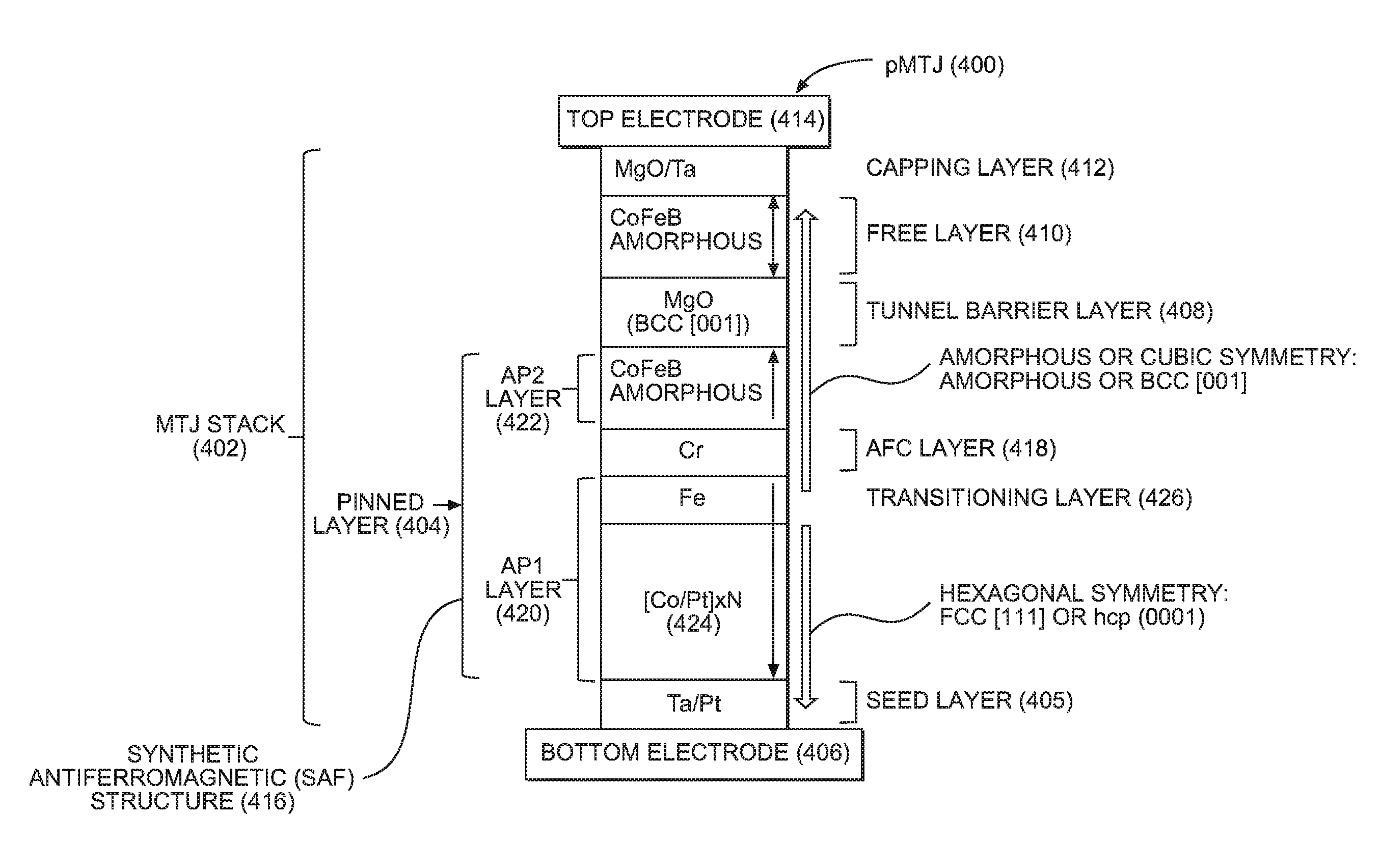
[0035]Aspects of the present disclosure involve perpendicular magnetic tunnel junction (pMTJ) devices employing a thin pinned layer stack with an thin upper anti-parallel (AP) layer (AP2 layer). Another aspect of the present disclosure involves employing a combination of materials in the pMTJ device for a bottom anti-parallel (AP) layer (AP1 layer) and an anti-ferromagnetic coupling (AFC) layer in the thin pinned layer stack providing a transitioning start to a body-centered cubic (BCC) crystalline / amorphous structure below an upper AP layer (AP2 layer). This can promote a high tunnel magnetoresistance ratio (TMR) with reduced pinned layer thickness. ...


PUM


Abstract

Perpendicular magnetic tunnel junction (pMTJ) devices employing a pinned layer stack with a thin top anti-parallel (AP2) layer and having a transitioning layer providing a transitioning start to a body-centered cubic (BCC) crystalline/amorphous structure below the top anti-parallel (AP2) layer, to promote a high tunnel magnetoresistance ratio (TMR) with reduced pinned layer thickness are disclosed. A first anti-parallel (AP) ferromagnetic (AP1) layer in a pinned layer has a face-centered cubic (FCC) or hexagonal closed packed (HCP) crystalline structure. A transitioning material (e.g., Iron (Fe)) is provided in a transitioning layer between the AP1 layer and an AFC layer (e.g., Chromium (Cr)) that starts a transition from a FCC or HCP crystalline structure, to a BCC crystalline/amorphous structure. In this manner, a second AP ferromagnetic (AP2) layer disposed on the AFC layer can be provided in a reduced thickness BCC crystalline or amorphous structure to provide a high TMR with a reduced pinned layer thickness.

Description

BACKGROUND[0001]I. Field of the Disclosure[0002]The technology of the disclosure relates generally to the structure of magnetic tunnel junction (MTJ) devices that can be used, for example, in magnetic random access memory (MRAM) for storage of data.[0003]II. Background[0004]Semiconductor storage devices are used in integrated circuits (ICs) in electronic devices to provide data storage. One example of a semiconductor storage device is a magnetic random access memory (MRAM). MRAM is non-volatile memory in which data is stored by programming a magnetic tunnel junction (MTJ) as part of an MRAM bit cell. One advantage of an MRAM is that MTJs in MRAM bit cells can retain stored information even when power is turned off. Data is stored in the MTJ as a small magnetic element rather than as an electric charge or current.[0005]In this regard, FIG. 1 is an illustration of an MTJ 100 provided in an MRAM bit cell to store data as a function of magnetization directions of two (2) layers in the M...

Claims


Application Information

Patent Timeline
IPC IPC(8): H01L29/66H01L43/12H01L43/02G11C11/16H01L43/10H01L43/08H01L27/22
CPCH01L27/228H01L43/08H01L43/10H01L43/12H01L43/02G11C11/161H01L28/00H10N50/85H10N50/10H10B43/27H10B61/22H10N50/01H10N50/80
Inventor GOTTWALD, MATTHIAS GEORGKAN, JIMMY JIANANPARK, CHANDOZHU, XIAOCHUNKANG, SEUNG HYUK
Owner QUALCOMM INC
Why Eureka
Try Eureka