Electronic module and method of assembling the same

a technology of electronic modules and modules, applied in the field of electronic modules, can solve the problems of increasing inductive load and inductive losses, reducing the area required by the two components, and requiring additional electrical connections for modules with two or more semiconductor components

Active Publication Date: 2008-10-28
INFINEON TECH AG
View PDF5 Cites 22 Cited by
  • Summary
  • Abstract
  • Description
  • Claims
  • Application Information

AI Technical Summary

Benefits of technology

[0013]The electronic module includes at least one vertical semiconductor power switch and at least one vertical semiconductor diode. According to an exemplary embodiment of the invention, the module accommodates two semiconductor components by mounting the semiconductor diode on top of the semiconductor power switch to form a stack. Therefore, the lateral space required within the housing of the module is determined largely by the lateral size of the semiconductor power switch. Consequently, a given semiconductor power switch and semiconductor diode can be accommodated within a module that has a smaller package outline. Given the current demand for miniaturization of electronic modules, this is very advantageous. Alternatively, a larger semiconductor chip with a higher switching power may be accommodated within a particular package housing. A package of a certain size may then be provided with a higher power rating. This is advantageous for applications in which higher power is required within a pre-defined limited space.
[0084]This can be provided by the use of an electrically conductive spacer or a raised front side metallization which is disposed directly on the anode contact of the diode. The outer surface, provided by either the anode contact or the electrically conductive spacer, is mechanically attached to and electrically connected to the input contact of the semiconductor power switch by an electrically conductive bonding layer. The bonding layer may cover substantially the whole of the anode contact so as to produce a mechanically stable stack and a low electrical resistance bond.

Problems solved by technology

However, the manufacture of the semiconductor body including two or more different types of device is expensive.
However, this approach has the disadvantage that modules with two or more semiconductor components require additional electrical connections to electrically connect the different components.
This increases the inductive load and inductive losses and causes switching losses.
Additionally, two or more die attachment processes are required to mount the dies next to each other on the die pad so that the assembly process is more complicated.
The plurality of semiconductor components also requires a certain minimum area within the package housing not only due to the size of the components themselves, but also due to the space required by the two die attachment processes.
The size to which the package housing of the module can be reduced is, therefore, limited.

Method used


Image

  • Electronic module and method of assembling the same
  • Electronic module and method of assembling the same
  • Electronic module and method of assembling the same

Examples


Embodiment Construction

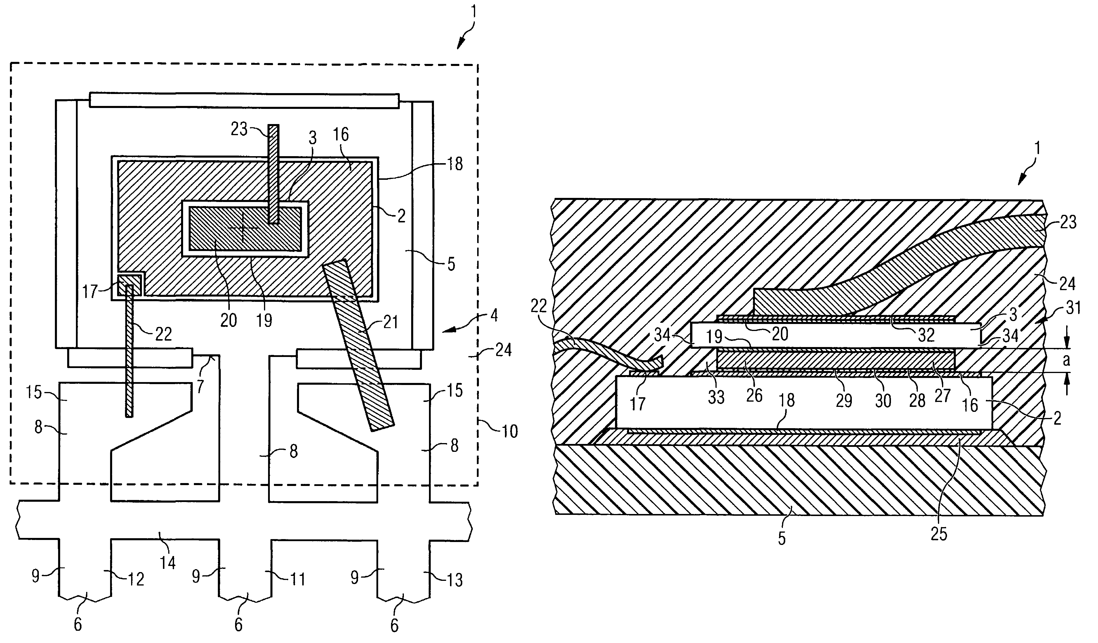
[0091]FIG. 1 shows an electronic module 1 according to a first embodiment of the invention which comprises a vertical MOSFET device 2, which provides a semiconductor power switch, and a vertical Schottky semiconductor diode 3. The electronic module 1 further comprises a leadframe 4 and package housing 10, which is indicated in FIG. 1 by the dashed line.

[0092]The leadframe 4 comprises a die pad 5, which is essentially rectangular, and three leads, or pins 6 which are arranged adjacent the long side 7 of the die pad 5. Each lead 6 has an inner portion 8, which is disposed within the package housing 10 and an outer portion 9 which is integral with the inner portion and extends outside of the package housing 10. The outer portion 9 of the leads 6 enables the electronic component 1 to be mounted on an external higher level substrate such as a printed circuit board (which is not shown in the figures) and enables the MOSFET device 2 and diode 3 to be electrically accessed from the printed ...


PUM


Abstract

An electronic module includes a semiconductor power switch and a semiconductor diode. The lower side of the semiconductor power switch includes an output contact mounted on a die pad of a leadframe, and the upper side of the semiconductor power switch includes a control contact and an input contact. The anode contact of the semiconductor diode is disposed on and electrically connected to the input contact of the semiconductor power switch. The cathode contact of the diode is electrically connected with the output contact of the power semiconductor switch.

Description

FIELD OF THE INVENTION[0001]The invention relates to electronic modules, in particular to modules including at least one semiconductor power switch and at least one semiconductor diode, and to methods of assembling electronic modules.BACKGROUND[0002]Electronic circuits such as those used in switched mode applications and in control circuits for DC motors typically require a number of different semiconductor components such as transistor devices and semiconductor diodes. The circuit is typically provided by one or more electronic modules, each module typically including a number of devices. A number devices may be provided within a single module in various ways.[0003]In one approach, a single semiconductor body is provided which includes both transistor structures and semiconductor diode structures. This arrangement has the advantage that the space required by the circuit is reduced. However, the manufacture of the semiconductor body including two or more different types of device is...

Claims


Application Information

Patent Timeline
Patent Type & Authority Patents(United States)
IPC IPC(8): H01L23/495
CPCH01L23/49513H01L23/49524H01L23/49562H01L23/49575H01L24/33H01L24/40H01L24/41H01L24/49H01L24/73H01L24/83H01L24/32H01L24/45H01L2224/45015H01L2224/45124H01L2224/45144H01L2224/48091H01L2224/48247H01L2224/48472H01L2224/4903H01L2224/49051H01L2224/49171H01L2224/49175H01L2224/73265H01L2224/83801H01L2224/8382H01L2924/01005H01L2924/01013H01L2924/01028H01L2924/01029H01L2924/01047H01L2924/0105H01L2924/01078H01L2924/01079H01L2924/01082H01L2924/01327H01L2924/13055H01L2924/13091H01L2924/19043H01L2924/20757H01L2924/2076H01L2924/30107H01L2924/0132H01L2224/32245H01L24/48H01L2224/2919H01L2924/01006H01L2924/01023H01L2924/01033H01L2924/01068H01L2924/014H01L2924/0665H01L2224/29111H01L2924/15747H01L2924/1305H01L2924/12032H01L2924/00014H01L2924/00H01L2924/3512H01L2224/0603H01L2224/40225H01L2224/40245H01L2924/12043H01L2924/181H01L2224/8381H01L2224/83825H01L2224/37144H01L2224/84801H01L24/37H01L2224/2612H01L2224/73221H01L2924/00012
Inventor OTREMBA, RALF
Owner INFINEON TECH AG
Why Eureka
Try Eureka