System and method for employing patterning process statistics for ground rules waivers and optimization

a technology of process statistics and ground rules, applied in the field of system and method for employing patterning process statistics for ground rules waiver and optimization, can solve the problems of design complexity and greater problem of design density, and achieve the effect of optimizing the rules for complian

Inactive Publication Date: 2008-11-04
GLOBALFOUNDRIES INC
View PDF25 Cites 9 Cited by
  • Summary
  • Abstract
  • Description
  • Claims
  • Application Information

AI Technical Summary

Problems solved by technology

Calculating 2-dimensional and intra-level intersect areas for structures in a semiconductor design remains a challenge within the semiconductor industry.
However, as the industry advances, designs have become more complex and design density has become a greater issue.

Method used


Image

  • System and method for employing patterning process statistics for ground rules waivers and optimization
  • System and method for employing patterning process statistics for ground rules waivers and optimization
  • System and method for employing patterning process statistics for ground rules waivers and optimization

Examples


Embodiment Construction

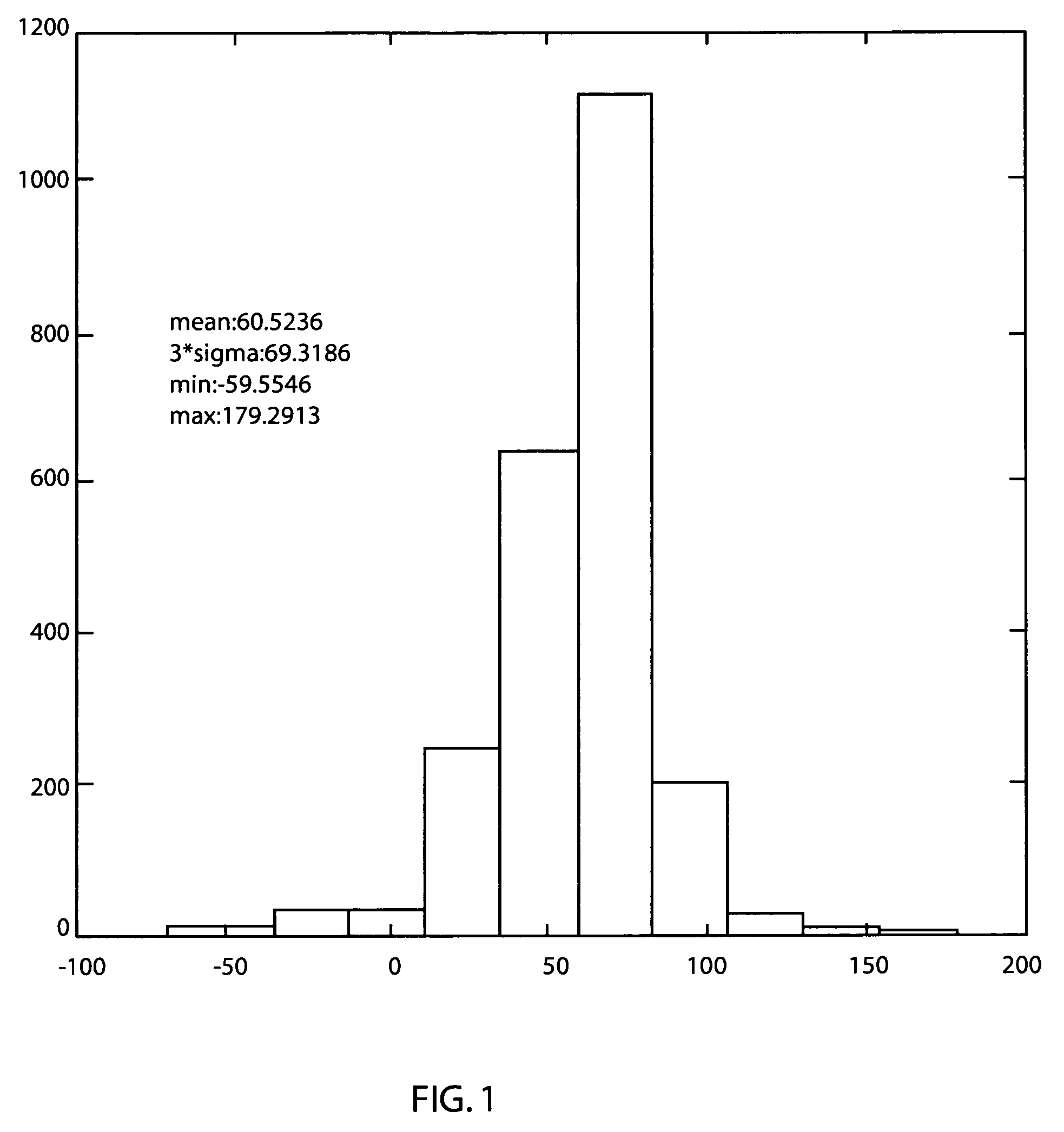
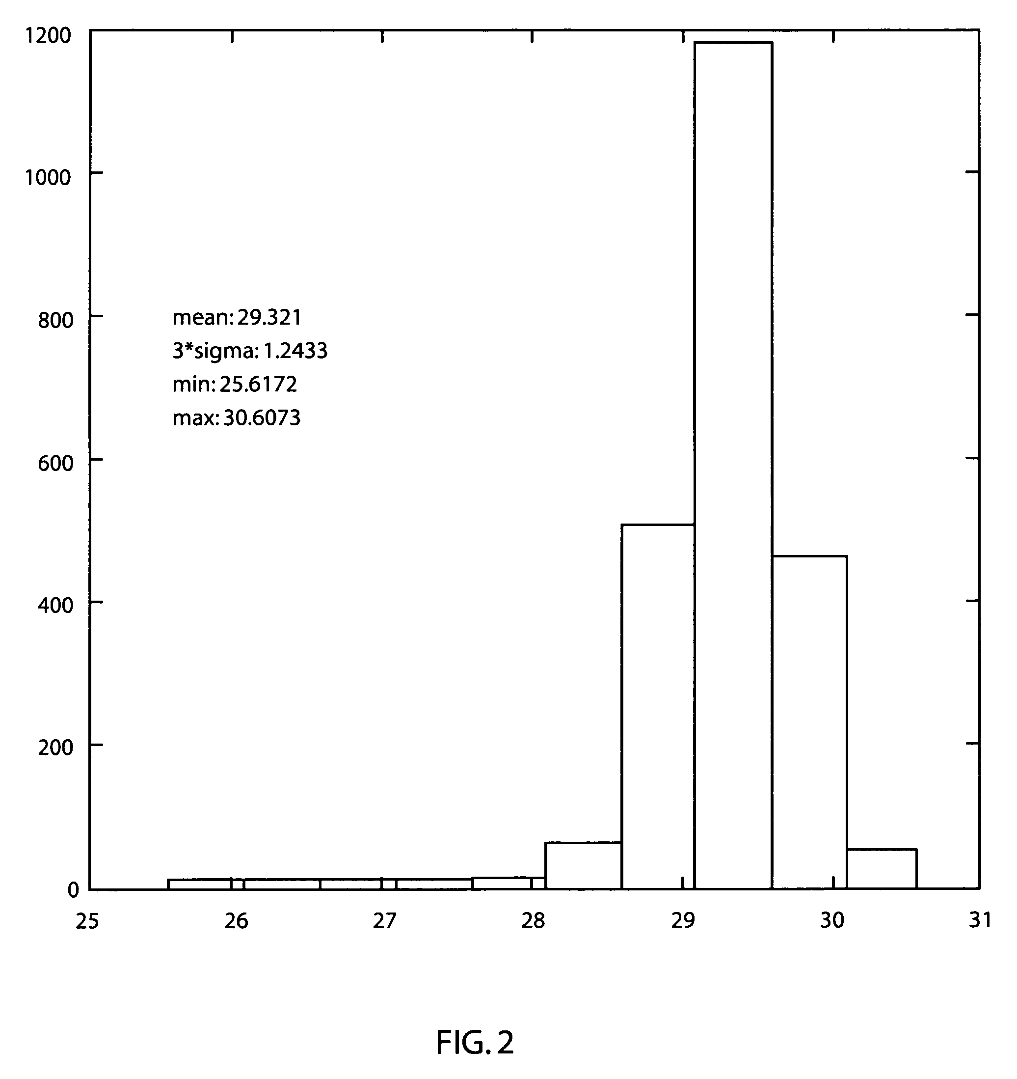
[0020]Embodiments in accordance with present principles provide a design or analytical tool that addresses layout considerations and intersection area computations for advanced technologies in semiconductor processes. In one embodiment, Optical Proximity Correction (OPC), lithography and non-lithography biases and non-linear critical dimension (CD) tolerances are combined in the same tool.

[0021]This tool successfully meets the needs of the semiconductor industry by permitting accurate analysis of complicated, intra-level design layout intersect areas, using production-level OPC which is targeted for the levels being analyzed. OPC includes modifying layout geometries for systematic distortions introduced during fabrication. The OPC tools employ non-printable modifications to a mask or other components to provide desired images for lithography. The intersect area computations from imaged features on the mask, for example, facilitate design rules or ground rules waivers and optimizatio...


PUM

PropertyMeasurementUnit
Optical Proximity Correctionaaaaaaaaaa
areaaaaaaaaaaa
areasaaaaaaaaaa

Abstract

A system and method of employing patterning process statistics to evaluate layouts for intersect area analysis includes applying Optical Proximity Correction (OPC) to the layout, simulating images formed by the mask and applying patterning process variation distributions to influence and determine corrective actions taken to improve and optimize the rules for compliance by the layout. The process variation distributions are mapped to an intersect area distribution by creating a histogram based upon a plurality of processes for an intersect area. The intersect area is analyzed using the histogram to provide ground rule waivers and optimization.

Description

BACKGROUND[0001]1. Technical Field[0002]The present invention relates to semiconductor chip design, and more particularly to a design tool for optimizing and providing ground rules waivers for chip designs and fabrication procedures.[0003]2. Description of the Related Art[0004]Calculating 2-dimensional and intra-level intersect areas for structures in a semiconductor design remains a challenge within the semiconductor industry. Intersect areas refer to areas common to a pair of layers in layouts of devices or components on a semiconductor chip. These areas are constrained by ground rules which provide requirements for spacings between the components, the component sizes, etc.[0005]Ground rules are restrictions with regard to the geometry of the layout that must be adhered to by the designer of a Very Large Scale Circuit (VLSI) chip. Examples of ground rules are minimum width of a channel, minimum distance between two corners, minimum distance between two features and the like, as is...

Claims


Application Information

Patent Timeline
Patent Type & Authority Patents(United States)
IPC IPC(8): G06F17/50G03F1/00G06F19/00G21K5/00G06F40/00
CPCG06F17/5068G06F30/39
Inventor HENG, FOOK-LUENLAVIN, MARK ALANLEE, JIN-FUWLIN, CHIEH-YUNAYAK, JAWAHAR PUNDALIKSINGH, RAMA NAND
Owner GLOBALFOUNDRIES INC
Why Eureka
Try Eureka