Molecular glass photoresists

a technology of photoresisting and glass, applied in the field of molecular glass photoresisting, can solve the problems of inability to achieve sub-200 nm exposures, short wavelength resists, and general unsuitability for sub-200 nm exposures, and achieve the effect of transparent glasses at shorter wavelengths

Inactive Publication Date: 2008-11-18
CORNELL RES FOUNDATION INC
View PDF0 Cites 2 Cited by
  • Summary
  • Abstract
  • Description
  • Claims
  • Application Information

AI Technical Summary

Benefits of technology

[0040]In a refinement, transparency of the disclosed glasses at shorter wavelengths, such as the EUV wavelength of 13.4 nm, may be enhanced by incorporation of low absorbing atoms such as C, H and Si.

Problems solved by technology

The manufacture of integrated circuit devices with smaller features introduces new challenges in many of the fabrication processes conventionally used in semiconductor fabrication.
Even shorter wavelength resists, such as those effective at 248 nm exposures, also are generally unsuitable for sub-200 nm exposures, such as 193 nm.
For example, current photoresists can be highly opaque to short exposure wavelengths such as 193 nm, thereby resulting in poorly resolved images.
However, as will be discussed below, other features of the projection lithography process have impeded the use of shorter wavelengths.
Unfortunately, most photoresist materials absorb extreme ultraviolet (EUV) radiation strongly in the range of 4.5-15 nm.
While this is advantageous from the standpoint of resist speed (i.e. the exposure dose required to form a pattern) and the associated printing rate, it poses a serious problem for projection lithographic methods that employ EUV radiation because of highly nonuniform absorption of this radiation through the photoresist thickness.

Method used


Image

  • Molecular glass photoresists
  • Molecular glass photoresists
  • Molecular glass photoresists

Examples


Embodiment Construction

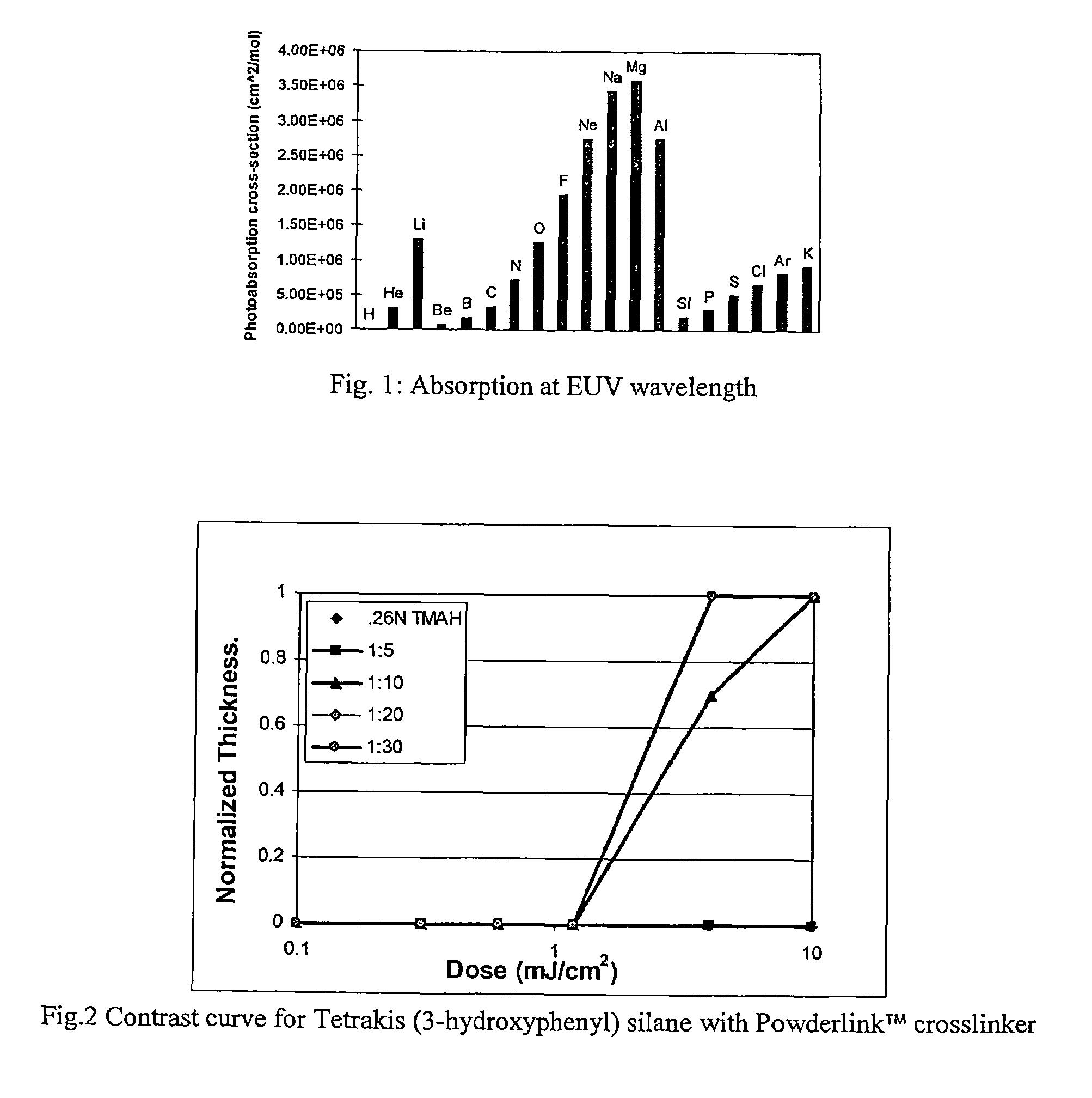
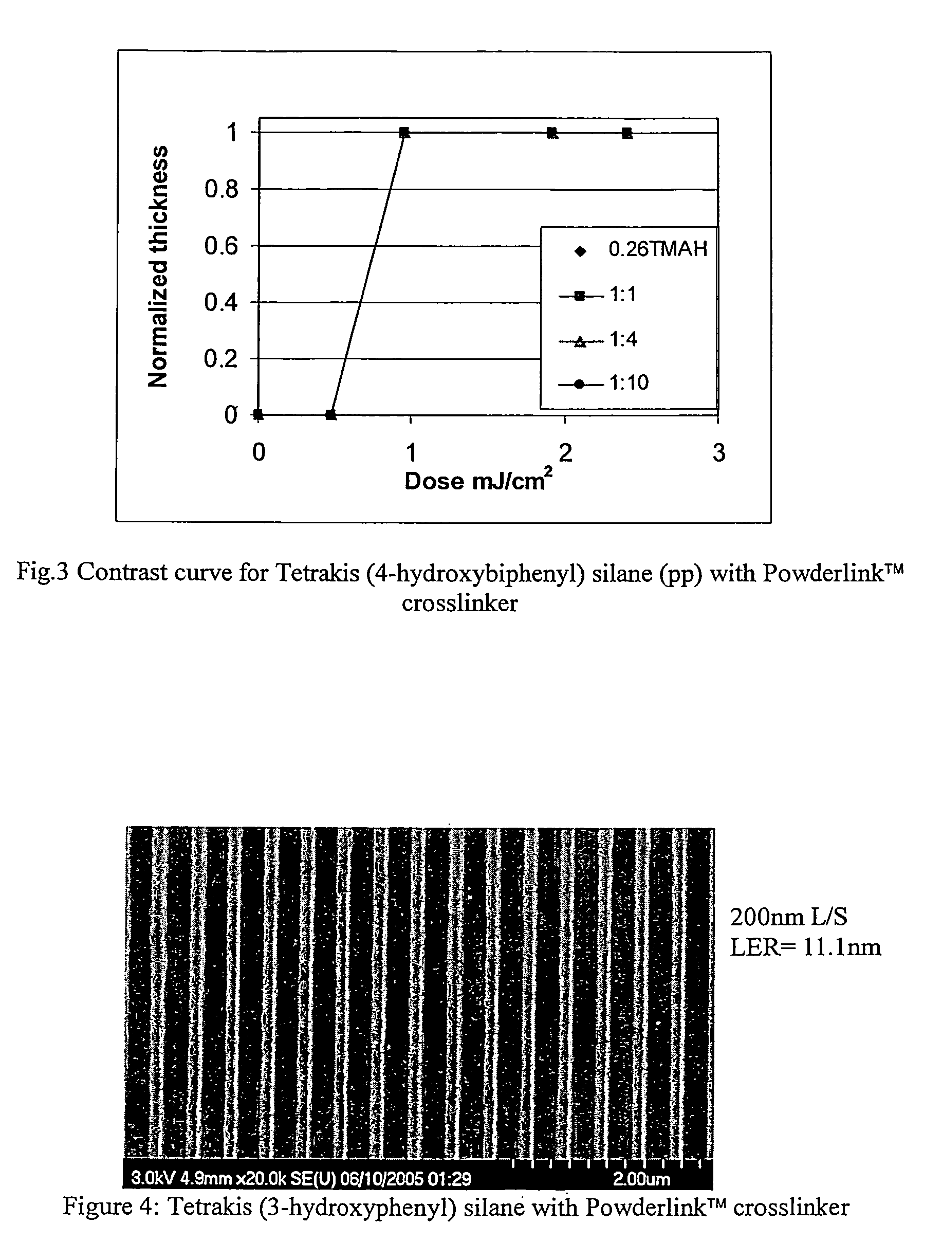
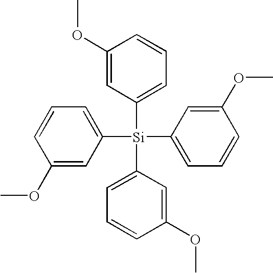
[0048]The disclosed molecular glass photoresists combine the beneficial aspects of small molecules along with many of the favorable aspects of polymers. The disclosed molecular glass photoresists have a well defined structure without poorly defined end group locations. The disclosed molecular glass photoresists can be purified using standard chromatographic techniques.

[0049]Unlike other small molecules, the unique glass forming properties of the disclosed molecular glass photoresists stem from an inability to crystallize. Thus, the disclosed molecules can be trapped in a kinetically stable amorphous state. Like polymers, the disclosed molecular glasses demonstrate glass transition temperatures (Tg) significantly higher than room temperature despite their modest molecular dimensions. The disclosed glass photoresists can be characterized by the disorder in both intermolecular distance and orientation and the presence of free volume. Unlike single crystals and liquid crystalline materi...


PUM

PropertyMeasurementUnit
wavelengthaaaaaaaaaa
exposure wavelengthsaaaaaaaaaa

Abstract

Several small molecule, molecular glasses are disclosed with new architectures designed for use as photoresists in semiconductor lithography. The disclosed photoresists are low molecular weight organic materials that demonstrate a glass transition temperature significantly above room temperature as well as a low tendency towards crystallization. The molecular glass photoresists have a tetrahedral silane molecular core with four phenyl groups or four biphenyl groups. Each phenyl group or each outer phenyl group of a biphenyl group has a methoxy or hydroxy group at the 3- or 4-position. For the biphenyl embodiments, the linkage may be meta-meta, meta-para, para-para or para-meta.

Description

BACKGROUND[0001]1. Technical Field[0002]Molecular glass photoresists are disclosed for use in semiconductor lithography processes. The disclosed molecular glass photoresists include a tetrahedral structure comprising a silicon core atom with sp3 orbitals of the silicon core atom. The tetrahedral structure of the disclosed glass resists provides a diamond-like 3-D architecture, a glass transition temperature (Tg) well above room temperature and excellent glass forming properties without the need to incorporate Tg-suppressing aliphatic chains to prevent crystallinity.[0003]2. Description of the Related Art[0004]To meet the requirements for faster performance, integrated circuit devices continue to get smaller and smaller. The manufacture of integrated circuit devices with smaller features introduces new challenges in many of the fabrication processes conventionally used in semiconductor fabrication. One fabrication process that is particularly impacted is photolithography.[0005]In sem...

Claims


Application Information

Patent Timeline
Patent Type & Authority Patents(United States)
IPC IPC(8): G03C1/00
CPCG03F7/038G03F7/0755
Inventor DE SILVA, EKMINI ANUJAFORMAN, DREW C.OBER, CHRISTOPHER K.
Owner CORNELL RES FOUNDATION INC
Why Eureka
Try Eureka