Embedded metal heat sink for semiconductor device and method for manufacturing the same

a technology of opto-electric devices and heat sinks, which is applied in the direction of semiconductor lasers, semiconductor/solid-state device details, lasers, etc., can solve the problems of degrading the operational quality of the module, burning out the opto-electrical devices, flickering lights, etc., to achieve the effect of prolonging the life of the device, enhancing the heat-sink efficiency, and enhancing the stability of the devi

Inactive Publication Date: 2008-11-18
NAT CHENG KUNG UNIV
View PDF13 Cites 1 Cited by
  • Summary
  • Abstract
  • Description
  • Claims
  • Application Information

AI Technical Summary

Benefits of technology

[0007]One aspect of the present invention is to provide an embedded metal heat sink for a semiconductor device, in which the embedded metal heat sink includes at least one bonding pad used as a transition electrode for electrically connecting a positive electrode or a negative electrode of the semiconductor device and an outer circuit, so that the semiconductor device embedded on the metal heat sink can be successfully connected to the outer circuit.
[0008]Another aspect of the present invention is to provide a method for manufacturing an embedded metal heat sink for a semiconductor device, in which the metal heat sink can be directly deposited on a bottom surface of the semiconductor device with the assistant of an adhesive tape and without the use of glue or a pasting technique. In addition, bonding pads are deposed on the metal heat sink surrounding the semiconductor device for the electrical transition between electrodes of the semiconductor device and an outer circuit. Therefore, the temperature of the operating device can be rapidly and effectively lowered for improving the operational quality of the device and prolonging the life of the device, and the positive electrode and the negative electrode of the semiconductor device can be successfully connected to the outer circuit, thereby saving the using of a circuit board.
[0012]A semiconductor device is directly embedded into a metal heat sink by directly forming the metal heat sink on the semiconductor device. Then, bonding pads are deposed on the metal heat sink around the semiconductor device for the transition of the electrical connection between the electrodes of the semiconductor device and an outer circuit. As a result, the metal heat sink cannot be additionally deposed on a circuit board, thereby greatly increasing the heat-sinking efficiency, enhancing the operation stability of the device and effectively prolonging the life of the device.

Problems solved by technology

However, when the opto-electrical devices are operated at high power, the temperature of the module composed of the opto-electrical devices increases, thereby degrading the operational quality of the module and ultimately burning out the opto-electrical devices.
However, regarding setting fans in the module, the vibration caused by the operation of the fans results in the lights flickering, and the fans consume additional power.
As a result, the heat generated during the operation of the opto-electrical device mostly accumulates at the connection interface, so that the heat sinks cannot transfer heat well, thereby making the heat sinks less effective, and easily damaging the opto-electrical devices during long-term operation or ultimately making the opto-electrical devices being operated with larger input power usage.
Accordingly, the heat generated during the operation of the device accumulates at the glue, and the thermal conductivity of the circuit board composed of the plastic material is low, so the heat conductivity rate is low and greatly decreases the heat dissipation efficiency of the heat sinks.

Method used


Image

  • Embedded metal heat sink for semiconductor device and method for manufacturing the same
  • Embedded metal heat sink for semiconductor device and method for manufacturing the same
  • Embedded metal heat sink for semiconductor device and method for manufacturing the same

Examples


Embodiment Construction

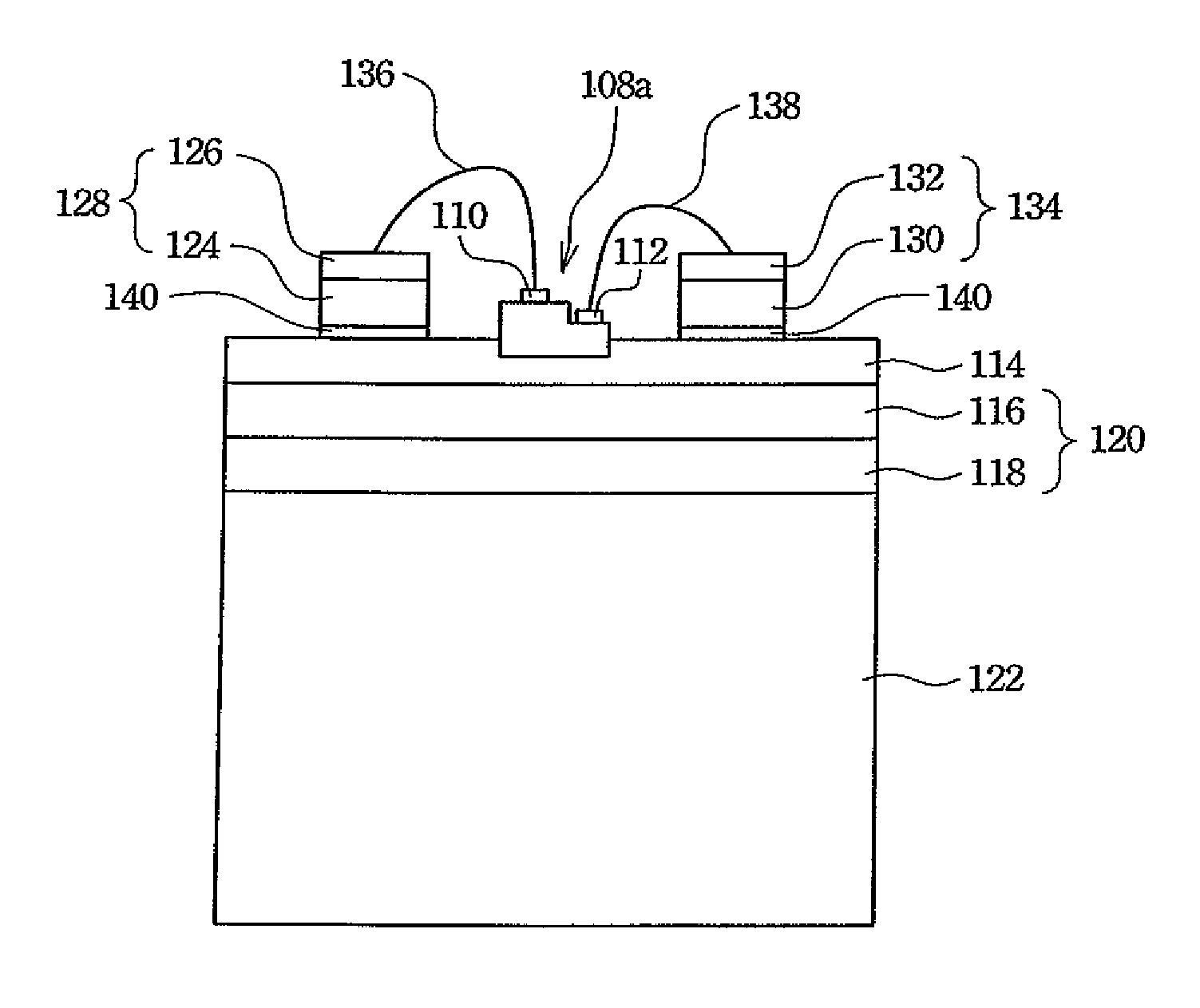
[0015]The present invention discloses an embedded metal heat sink for a semiconductor device and a method for manufacturing the same, in which electrodes of the semiconductor device are in contact with an outer circuit, and the heat-sinking efficiency of the metal heat sink is increased to improve the heat-dissipating problem of the semiconductor device. In order to make the illustration of the present invention more explicit, the following description is stated with reference to FIGS. 1A through 8.

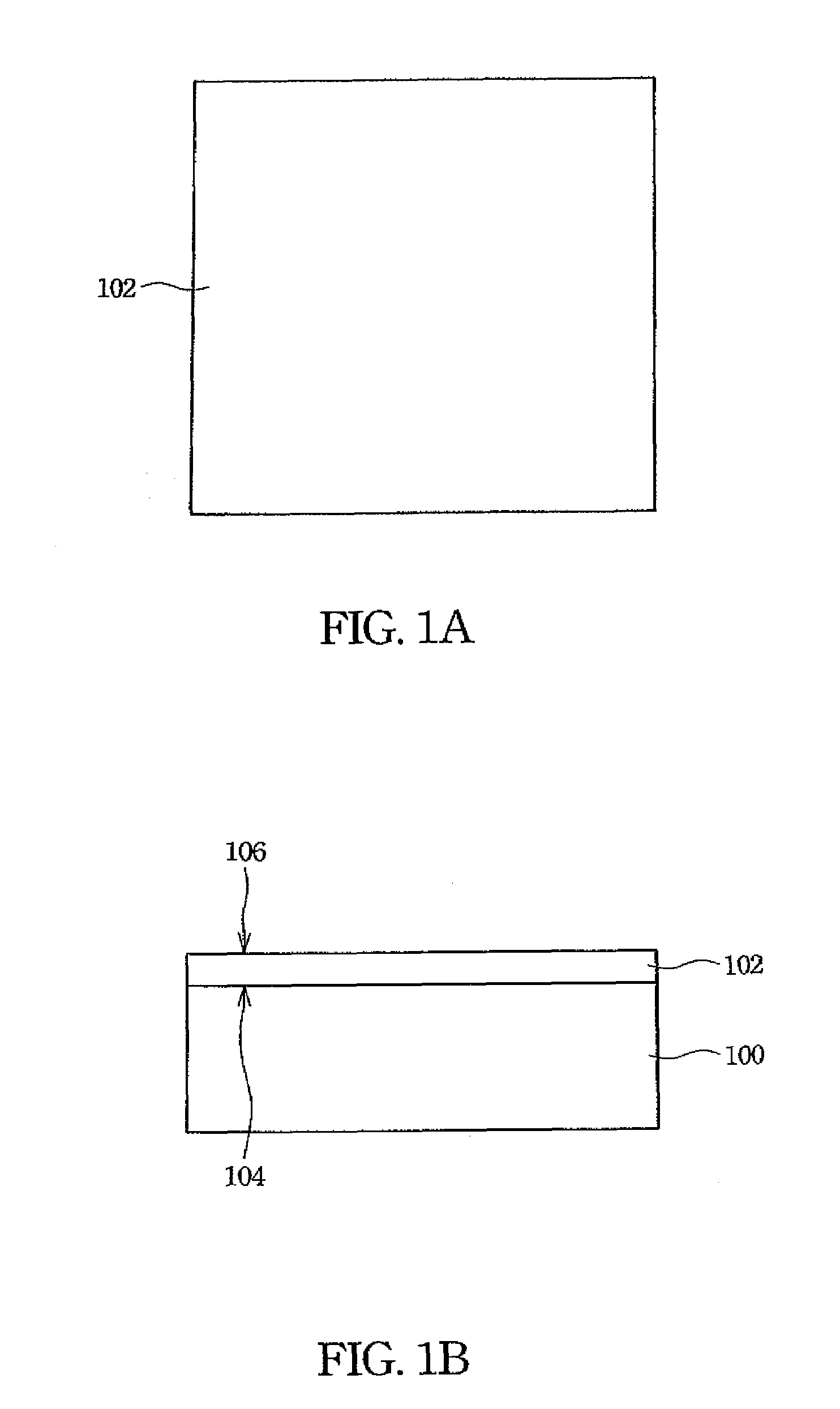
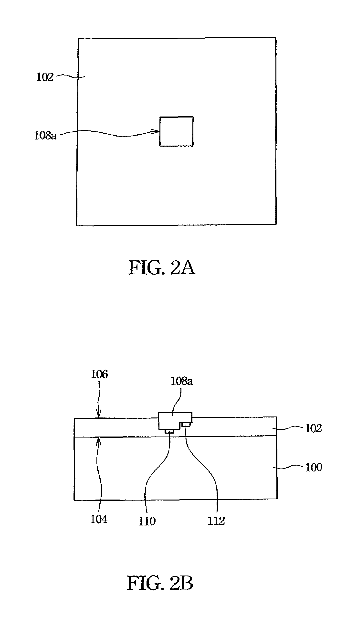
[0016]FIGS. 1A through 8 are schematic flow diagrams showing the process for manufacturing an embedded metal heat sink for a semiconductor device in accordance with a preferred embodiment of the present invention, wherein the schematic flow diagrams includes cross-sectional views and the corresponding top views. In the manufacturing of an embedded metal heat sink of a semiconductor device of the present invention, a temporary substrate 100 and an adhesive tape 102 are initially provided, ...


PUM

PropertyMeasurementUnit
thicknessaaaaaaaaaa
thicknessaaaaaaaaaa
thicknessaaaaaaaaaa

Abstract

An embedded metal heat sink for a semiconductor device and a method for manufacturing the same are described. The embedded metal heat sink for a semiconductor device comprises a metal thin layer, a metal heat sink and two bonding pads. The metal thin layer including a first surface and a second surface on opposite sides, wherein at least one semiconductor device is embedded in the first surface of the metal thin layer, and the semiconductor device has two electrodes with different conductivity types. The metal heat sink is deposited on the second surface of the metal thin layer. The bonding pads are deposed on the first surface of the metal thin layer around the semiconductor device and are respectively corresponding to the electrodes, wherein the electrodes are electrically and respectively connected to the corresponding bonding pads by at least two wires, and the bonding pads are electrically connected to an outer circuit.

Description

RELATED APPLICATIONS[0001]The present application is based on, and claims priority from, Taiwan Application Serial Number 95123020, filed Jun. 26, 2006, the disclosure of which is hereby incorporated by reference herein in its entirety.FIELD OF THE INVENTION[0002]The present invention relates to a metal heat sink and a method for manufacturing the same, and more particularly, to an embedded metal heat sink for an opto-electrical device and a method for manufacturing the same.BACKGROUND OF THE INVENTION[0003]When small solid state opto-electrical devices, such as light-emitting diodes (LEDs) or laser diodes (LDs), are applied in a large or small backlight module or illumination module, many opto-electrical devices are needed to generate sufficient brightness or illumination for the modules. However, when the opto-electrical devices are operated at high power, the temperature of the module composed of the opto-electrical devices increases, thereby degrading the operational quality of ...

Claims


Application Information

Patent Timeline
Patent Type & Authority Patents(United States)
IPC IPC(8): H01L21/44H01L21/48H01L33/62H01L33/64
CPCH01L33/641H01L33/60H01L33/62H01L2224/48091H01L2224/49107H01L2924/01078H01L2924/01079H01S5/0226H01S5/02276H01S5/02469H01L2924/00014H01S5/02345H01S5/0236H01L23/36
Inventor SU, YAN-KUINCHEN, KUAN-CHUNLIN, CHUN-LIANGHUANG, JIN-QUANHU, SHU-KAI
Owner NAT CHENG KUNG UNIV
Why Eureka
Try Eureka