Electron emitting device, electron source, image display apparatus and image receiving display apparatus

an electron emitting device and electron source technology, applied in the direction of discharge tube luminescnet screens, discharge tube/lamp details, discharge tube main electrodes, etc., can solve the problems of difficult to form circular cones or quadrangular pyramids easily, and achieve high resolution

Inactive Publication Date: 2008-11-25
CANON KK
View PDF11 Cites 13 Cited by
  • Summary
  • Abstract
  • Description
  • Claims
  • Application Information

AI Technical Summary

Benefits of technology

[0009]The present invention has been carried out in order to solve the above described problems, and an object of the invention is to constitute an electron emitting device capable of controlling the region of electrons reaching an anode electrode by a simple constitution.
[0011]According to the present invention, the electron emitting device of a simple constitution where the spots of electrons reaching the anode electrode are small can be realized. As a result, in the image display apparatus using the electron emitting device of the present invention, the image of high resolution can be displayed.

Problems solved by technology

However, there has been a problem in that it is difficult to form the circular cone or the quadrangular pyramid easily and with good reproducibility.

Method used


Image

  • Electron emitting device, electron source, image display apparatus and image receiving display apparatus
  • Electron emitting device, electron source, image display apparatus and image receiving display apparatus
  • Electron emitting device, electron source, image display apparatus and image receiving display apparatus

Examples


first embodiment

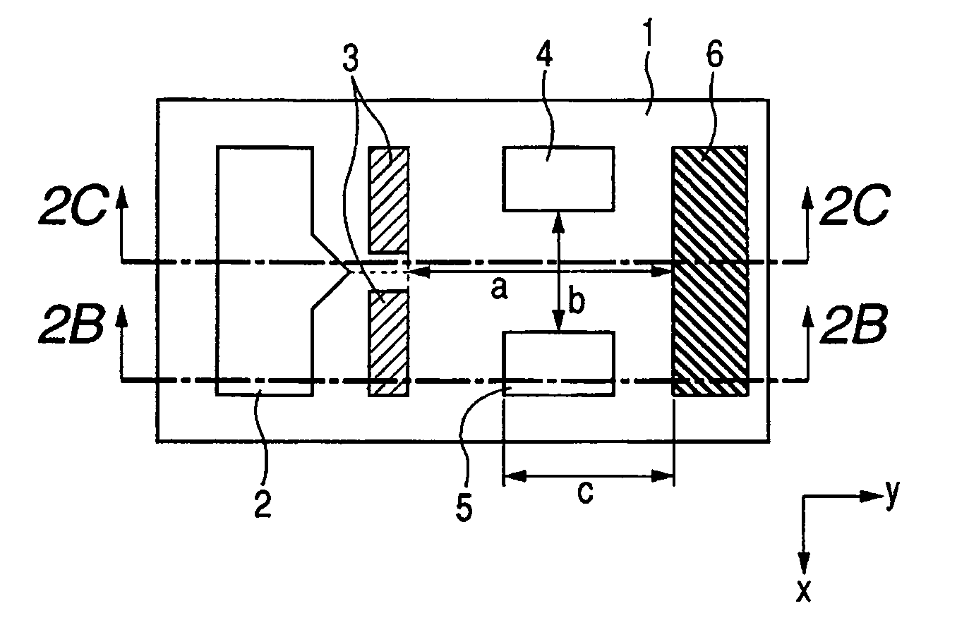
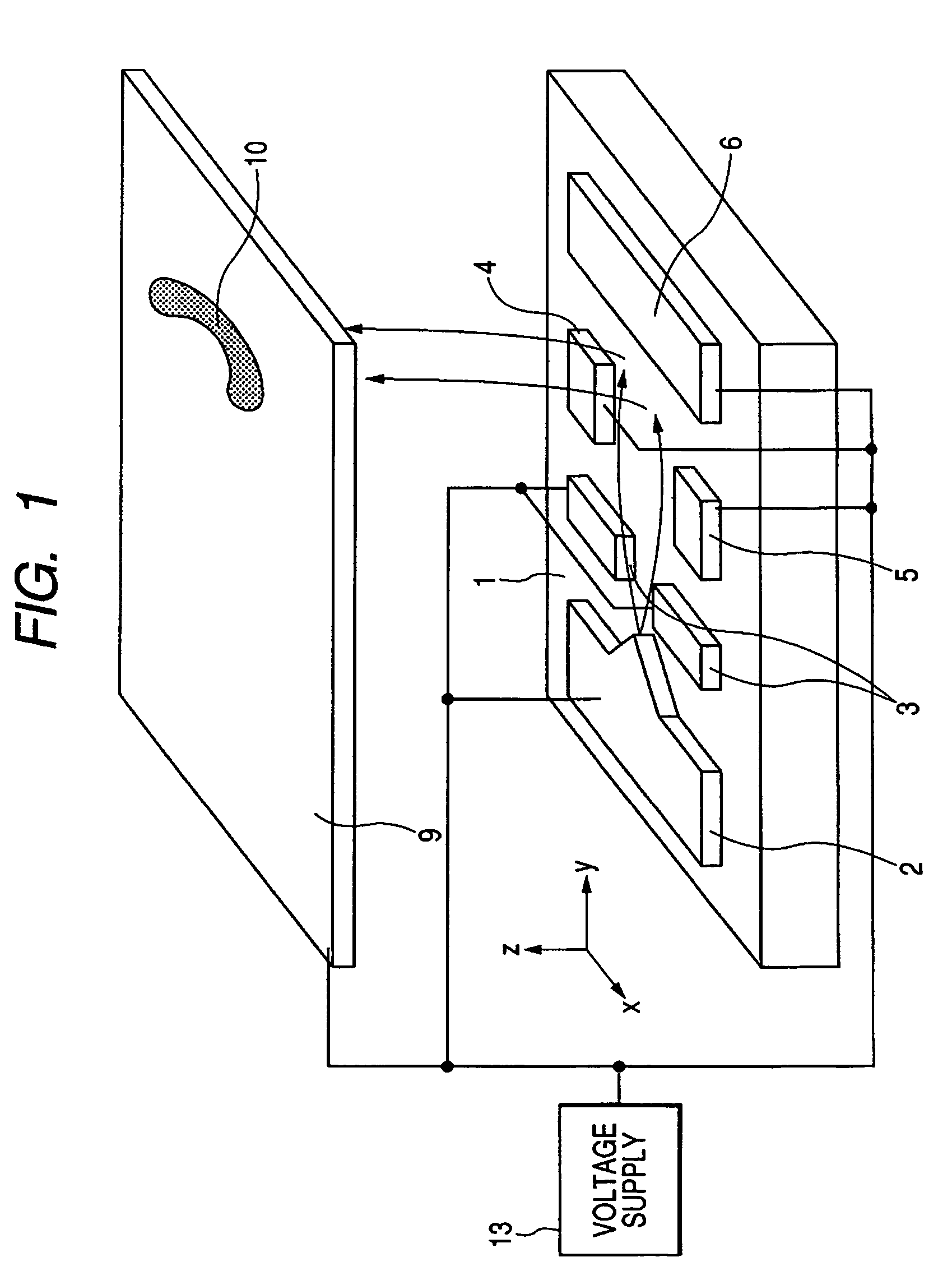
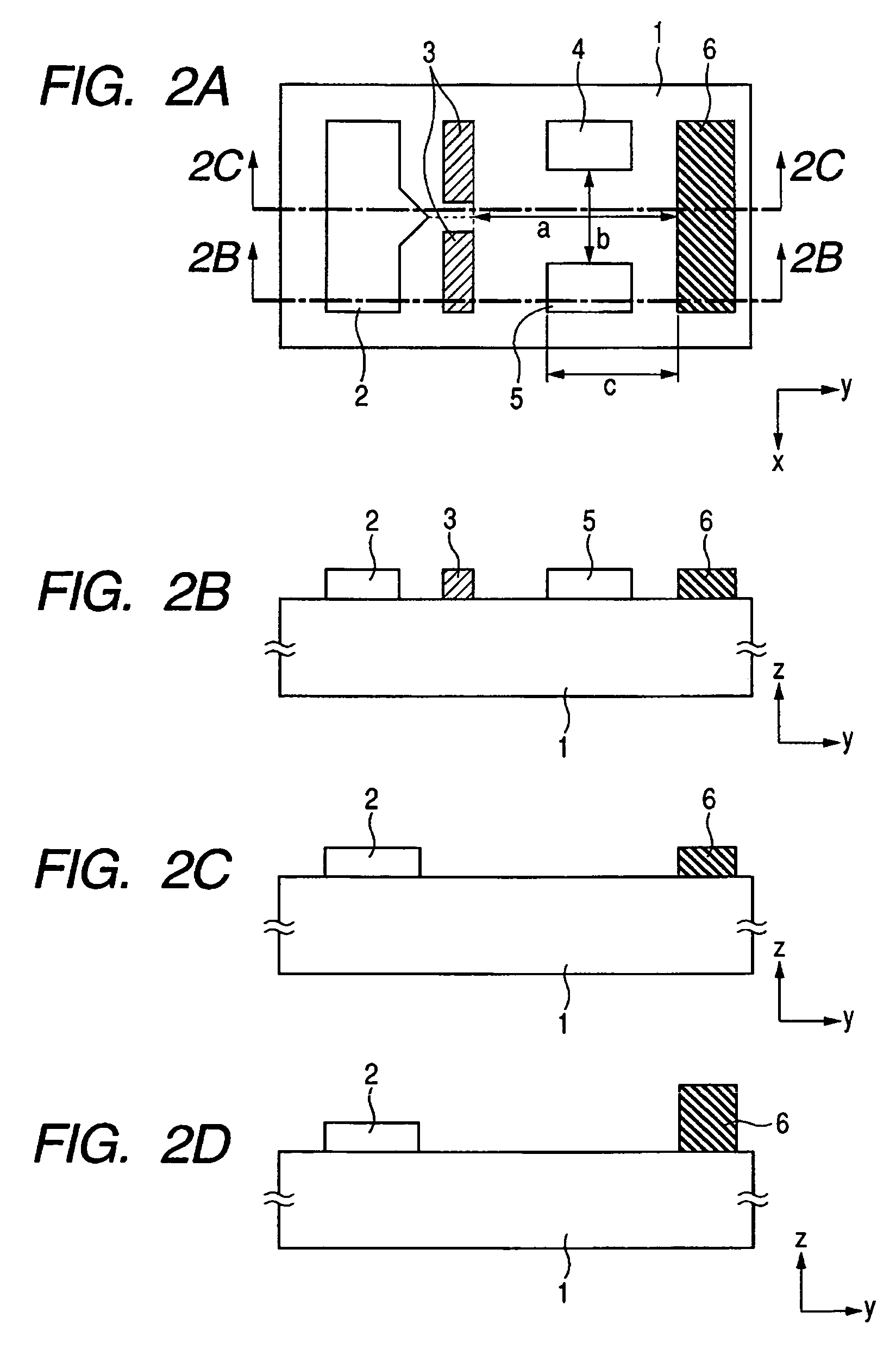
[0023]An electron emitting device according to a first embodiment of the present invention will be described by using a schematic illustration shown the FIG. 1. FIG. 1 shows an oblique view of the electron emitting device according to the present embodiment. In the Figure, reference numeral 1 denotes a substrate, reference numeral 2 denotes a cathode electrode, reference numeral 3 denotes an extraction electrode, reference numeral 4 denotes a first deflecting electrode, reference numeral 5 denotes a second deflecting electrode, reference numeral 6 denotes a third deflecting electrode, reference numeral 9 denotes an anode electrode, reference numeral 10 denotes an electron beam irradiating region, and reference numeral 13 denotes voltage supply means. Further, arrow marks in the Figure show the trajectories of the electrons emitted from the electron emitting portion of the cathode electrodes 2 at the driving time.

[0024]The electron emitting device of the present embodiment applies a ...

second embodiment

[0055]An electron emitting device according to a second embodiment of the present invention is schematically shown in FIGS. 4A, 4B and 4C.

[0056]The electron emitting device according to the present embodiment is the same as the electron emitting device according to the first embodiment except that one deflecting electrode is provided in place of the first deflecting electrode, the second deflecting electrode, and the third deflecting electrode. The same reference numerals are attached to the same constituent members. The portion different from the first embodiment will be described below.

[0057]FIG. 4A shows a top plan view of the electron emitting device according the present embodiment, and FIG. 4B shows a sectional view cut along the line 4B-4B of the FIG. 4A, and FIG. 4C shows a sectional view cut along the line 4C-4C of FIG. 4A. In FIGS. 4A to 4C, reference numeral 7 denotes a deflecting electrode, and reference numeral 11 denotes a deflecting region.

[0058]From among the end por...

third embodiment

[0062]An electron emitting device according to a third embodiment of the present invention is schematically shown in FIGS. 5A, 5B, and 5C.

[0063]The electron emitting device according to the present embodiment is the same as the electron emitting device according to the second embodiment except that, from among the end portion, at the side of an extraction electrode 3, of a cathode electrode 2, a portion is isolated from the extraction electrode 3 further than distant other portion, and the distant portion is provided with the electron emitting member 8. Consequently, the same constituent member is attached with the same reference numeral, and the portion different from the second embodiment will be described below.

[0064]FIG. 5A shows a top plan view of the electron emitting device according to the present embodiment, FIG. 5B shows a sectional view cut along the line 5B-5B of FIG. 5A, and FIG. 5C shows a sectional view cut along the line 5C-5C of FIG. 5A. In FIGS. 5A to 5C, reference...


PUM


Abstract

An electron emitting device comprising on a substrate: an electrode extracting electrons from the electron emitting portion, the electrode applied with a voltage higher then the cathode electrode; and an deflecting electrode deflecting the electrons extracted from the electron emitting portion by the extraction electrode, the deflecting electrode applied with the voltage lower than the voltage of the extraction electrode; wherein the electron emitting device is disposed so as to be opposed to an anode electrode, and the extraction electrode is disposed between the cathode electrode and the deflecting electrode, and wherein the deflecting electrode comprises a portion opposed to the electron emitting portion, and other portions disposed to nip a region between the electron emitting portion and said portion in a direction crossing the direction along which the portion and the electron emitting portion are opposed.

Description

BACKGROUND OF THE INVENTION[0001]1. Field of the Invention[0002]The present invention relates to an electron source, an image display apparatus, and an image receiving display apparatus, which are used for a TV receiver, a display device of a computer, an electron beam scribing apparatus, and the like.[0003]2. Related Background Art[0004]Heretofore, in general, as an electron emitting device, there has been a field emission electron emitting device.[0005]In one of the field emission electron emitting devices, there has been a so-called Spindt type electron emitting device where an electron emitting portion is shaped like a circular cone or a quadrangular pyramid in the direction vertical to a substrate surface.[0006]In the Spindt type electron emitting device, an electron emitting characteristic greatly depends on the shape of the circular cone or the quadrangular pyramid which is the electron emitting device. However, there has been a problem in that it is difficult to form the cir...

Claims


Application Information

Patent Timeline
Patent Type & Authority Patents(United States)
IPC IPC(8): H01J1/88H01J1/30
CPCH01J1/304H01J1/316H01J3/021H01J29/04H01J31/127H01J2201/316H01J2329/0407H01J2329/0486H01J2329/4604
Inventor NOMURA, KAZUSHINAKAJIMA, HIDEHIKO
Owner CANON KK
Why Eureka
Try Eureka