Method for manufacturing a semiconductor device

a manufacturing method and semiconductor technology, applied in the direction of semiconductor devices, basic electric elements, electrical appliances, etc., can solve the problems of electrode or the like corrosion, and the junction between the electrodes breaking

Inactive Publication Date: 2008-12-02
LAPIS SEMICON CO LTD
View PDF6 Cites 13 Cited by
  • Summary
  • Abstract
  • Description
  • Claims
  • Application Information

AI Technical Summary

Benefits of technology

[0014]Thus, the present invention is capable of obtaining advantageous effects in that a liquid resin can be injected into all spaces in one process at a time, the liquid resin can uniformly be charged into all the spaces, and an interface can be prevented from being formed between the post-curing liquid resins.
in that a liquid resin can be injected into all spaces in one process at a time, the liquid resin can uniformly be charged into all the spaces, and an interface can be prevented from being formed between the post-curing liquid resins.

Problems solved by technology

A problem arises in that, according to such a manufacturing method, after the liquid resin extruded from each space has been cured, the liquid resin extruded from the next space is superimposed thereon and cured, and when an interface is formed between these layers and peeling occurs in the interface, corrosion of electrodes or the like occurs due to moisture absorption from the peeled interface.
Also a problem arises in that moisture that remains at the peeled interface expands due to heating in a reflow process at secondary mounting of the semiconductor device, thereby causing breakage of a junction between the electrodes.
Further, a problem arises in that since the peeled interface has no bonding force, stress due to the difference in thermal expansion between a metal material and the cured liquid resin from heat generated by the semiconductor device occurs in the junction between the electrodes, thus causing breakage of the junction between the electrodes due to thermal cycles.
Furthermore, a problem arises in that since the liquid resin extruded from each space is cured and the liquid resin is superimposed thereon in turn to seal the spaces among the semiconductor elements or the like, the extruded liquid resin expands over the substrate in turn and a relatively large area for placing the extruded liquid resin is needed, thus making it difficult to bring a semiconductor device into lesser size.
A problem arises in that when one attempts to inject the liquid resin into the plural spaces one at a time in order to cope with such a problem, it is difficult to uniformly inject the liquid resin into the respective spaces even though the carrier is tilted about 15° from the horizontal, and a sealing failure occurs in each space in which the amount of injected the liquid resin is insufficient.

Method used


Image

  • Method for manufacturing a semiconductor device
  • Method for manufacturing a semiconductor device
  • Method for manufacturing a semiconductor device

Examples


first preferred embodiment

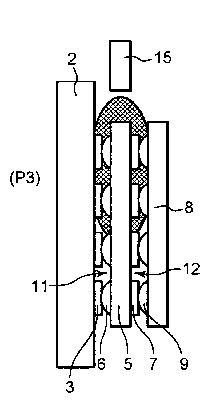
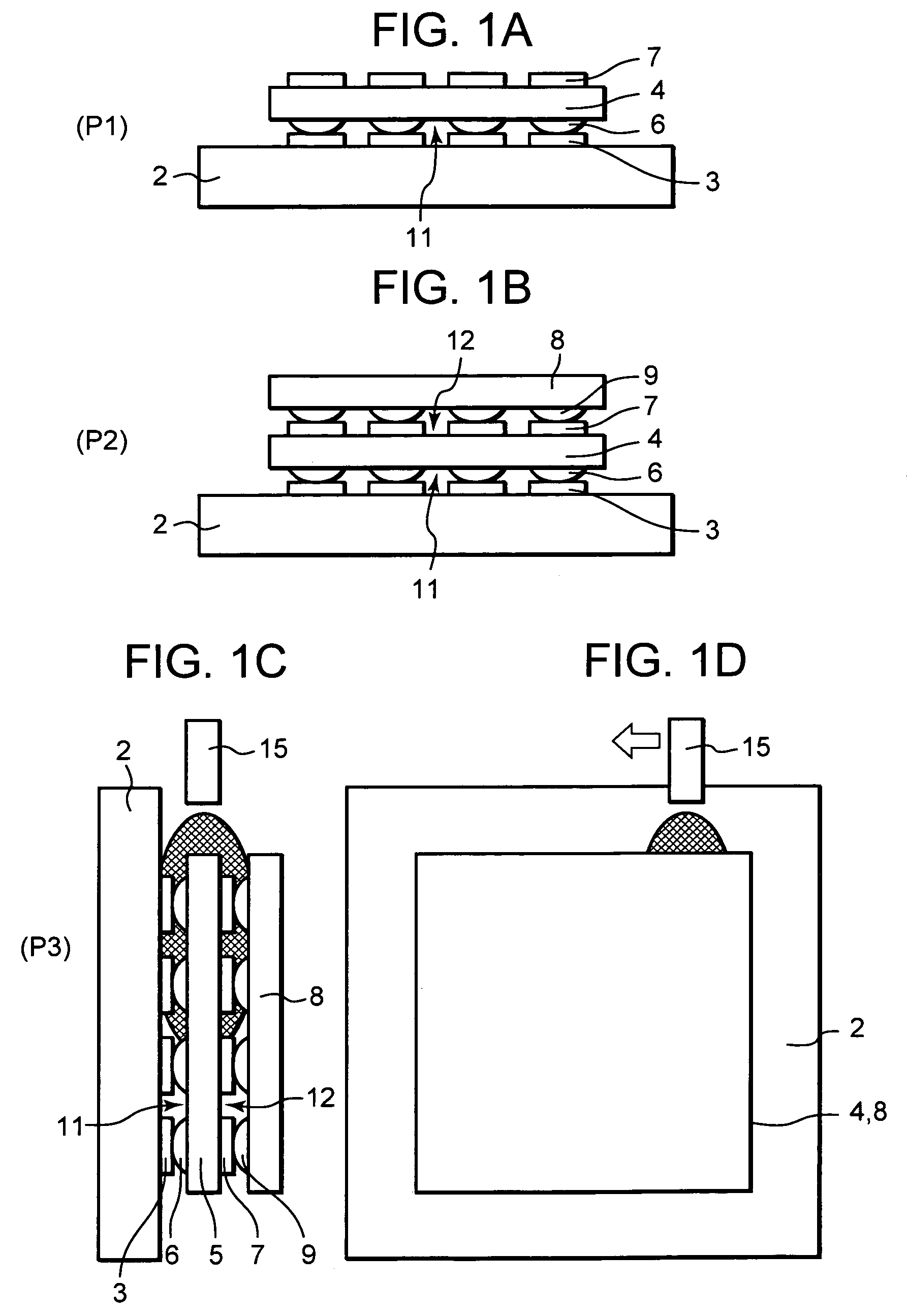
[0023]FIGS. 1A-1D show an explanatory diagram of a process for manufacturing a semiconductor device according to a first embodiment, and FIG. 2 is an explanatory diagram illustrating the semiconductor device according to the first embodiment, respectively.

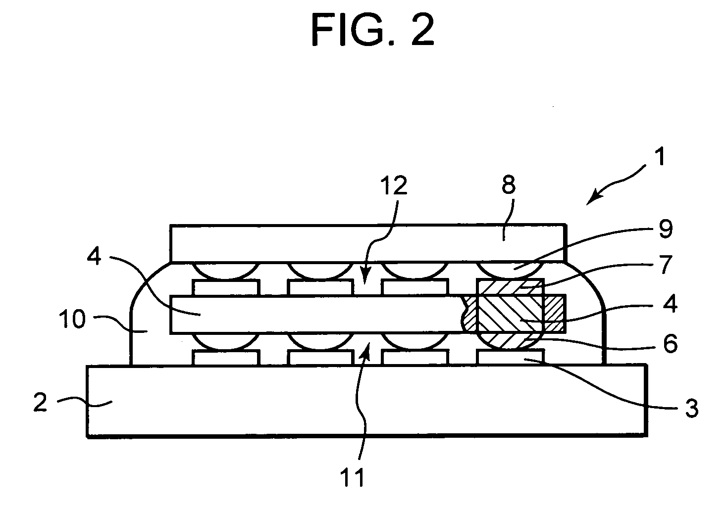
[0024]In FIG. 2, reference numeral 1 indicates the semiconductor device. The present embodiment shows a semiconductor device formed by stacking semiconductor elements on a substrate in two stages.

[0025]Reference numeral 2 indicates the substrate, which is a circuit substrate or a semiconductor element or the like. The substrate is provided with a plurality of ball pads 3 whose surfaces are plated with nickel or the like.

[0026]Reference numeral 4 indicates a first semiconductor element, which is a substantially square semiconductor element disposed in an intermediate stage. The first semiconductor element 4 is provided with bumps 6 formed by fusion-bonding solder or the like to ends on the front-face (corresponding to a surface on t...

second preferred embodiment

[0045]FIG. 3 is an explanatory diagram showing a process for manufacturing a semiconductor device according to a second embodiment.

[0046]Incidentally, portions similar to those employed in the first embodiment are given the same reference numerals and their explanations are omitted.

[0047]The semiconductor device 1 according to the present embodiment is similar to the first embodiment. A nozzle 15 is also similar in configuration to that employed in the first embodiment.

[0048]A method for manufacturing the semiconductor device according to the present embodiment in accordance with processes indicated by PA1-PA3 will be explained below using FIGS. 3A-3D.

[0049]Since the processes PA1 and PA2 of the present embodiment are similar to the processes P1 and P2 of the first embodiment, their explanations are omitted.

[0050]In the process PA3, a first semiconductor element 4 and a second semiconductor element 8 are bonded onto and stacked over a substrate 2 and formed in two stages. In such a ...

third preferred embodiment

[0057]FIGS. 4A-4D show an explanatory diagram of a process PB1-PB3 (part 1) for manufacturing a semiconductor device according to a third embodiment, and FIGS. 5A and 5B show an explanatory diagram of a process PB4 (part 2) for manufacturing the semiconductor device according to the third embodiment, respectively.

[0058]Incidentally, portions similar to those employed in the first embodiment are given the same reference numerals and their explanations are omitted.

[0059]The semiconductor device 1 according to the present embodiment is similar to that according to the first embodiment. A nozzle 15 is similar in configuration to that employed in the second embodiment.

[0060]In FIG. 4, reference numerals 20 indicate dam members, which are bank-shaped members for preventing an outflow of an underfill agent due to the extrusion of the underfill agent in the process of injecting the underfill agent. The dam members are formed by horizontally disposing a substrate 2 in a state in which first ...


PUM


Abstract

A method for manufacturing a semiconductor device formed by stacking a plurality of semiconductor elements on a substrate includes the steps of stacking the plurality of semiconductor elements on the substrate to form plural stages, placing the substrate substantially vertically and charging an underfill agent into spaces defined between the substrate and the corresponding semiconductor element and spaces defined among the stacked semiconductor elements through a nozzle from above side faces of the stacked semiconductor elements, and curing the charged underfill agent.

Description

BACKGROUND OF THE INVENTION[0001]1. Field of the Invention[0002]The present invention relates to a method for manufacturing a semiconductor device formed by stacking a plurality of semiconductor elements on a substrate.[0003]2. Description of the Related Art[0004]In a conventional method for manufacturing a semiconductor device, one semiconductor element is bonded face-down to electrodes provided on a carrier by means of its protruding electrodes. The carrier is tilted about 15° from the horizontal and a thermosetting liquid resin is injected into spaces between the carrier and the semiconductor element, which are defined by electrode bonding. Thereafter, the liquid resin is cured to seal the spaces defined by the electrode bonding, refer to, for example, Japanese Patent Application Laid-Open No. Hei 11 (1999)-354552, paragraphs 0022-0024 in the third page and FIG. 2.[0005]It has recently been practice to stack a plurality of semiconductor elements on a substrate, electrically bond ...

Claims


Application Information

Patent Timeline
Patent Type & Authority Patents(United States)
IPC IPC(8): H01L21/44
CPCH01L21/563H01L24/28H01L25/0657H01L2224/73203H01L2224/83102H01L2224/92125H01L2924/01015H01L2924/01029H01L2924/01078H01L2924/01082H01L2924/01006H01L2924/01023H01L2924/01033H01L2225/06517H01L2225/06513H01L2225/06541H01L2225/06565
Inventor SAEKI, YOSHIHIRO
Owner LAPIS SEMICON CO LTD
Why Eureka
Try Eureka