Light-emitting element having hole generating layer

a technology of light-emitting elements and hole generating layers, which is applied in the direction of discharge tubes/lamp details, organic semiconductor devices, discharge tubes/lamp details, etc., can solve the problems of reducing the service life of the device, and increasing the drive voltage. , to achieve the effect of suppressing the increase in the drive voltage over time, and reducing the cost of the devi

Active Publication Date: 2008-12-09
SEMICON ENERGY LAB CO LTD
View PDF38 Cites 100 Cited by
  • Summary
  • Abstract
  • Description
  • Claims
  • Application Information

AI Technical Summary

Benefits of technology

[0010]Consequently, it is an object of the present invention to provide a light-emitting element having a structure in which the increase in the drive voltage over time is small.
[0011]Further, it is an object of the present invention to provide a display device in which the drive voltage is low and the increase in the drive voltage over time is small and which can resist long-term use.
[0012]According to the present invention, a layer in contact with an electrode in a light-emitting element is a hole-generating layer such as a layer containing a P-type semiconductor or an organic compound layer containing a material having electron-accepting properties, a light-emitting layer is sandwiched between the hole-generating layers, and an electron-generating layer is formed between the hole-generating layer on a cathode side and the light-emitting layer. This enables the increase in the drive voltage over time to be small.
[0016]In a light-emitting element having a structure according to the present invention, the increase in the drive voltage over time can be suppressed.

Problems solved by technology

However, a material which can inject electrons comparatively easily from an electrode into a material mainly containing organic compound, or a material mainly containing organic compound which can transport electrons at a predetermined mobility or more are very limited.
This causes the problem that the drive voltage increases drastically over time.

Method used


Image

  • Light-emitting element having hole generating layer
  • Light-emitting element having hole generating layer
  • Light-emitting element having hole generating layer

Examples


embodiment mode 1

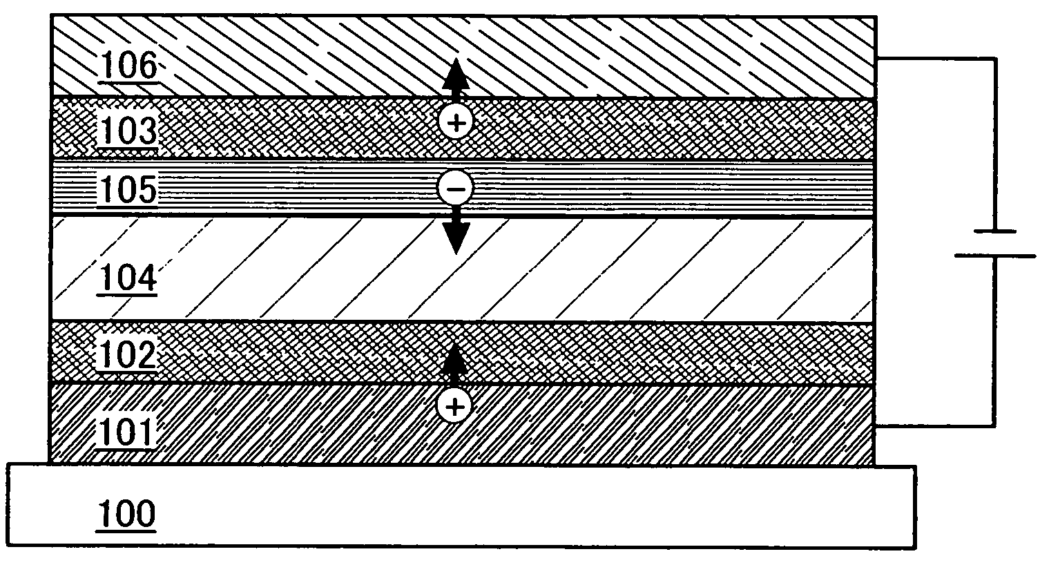
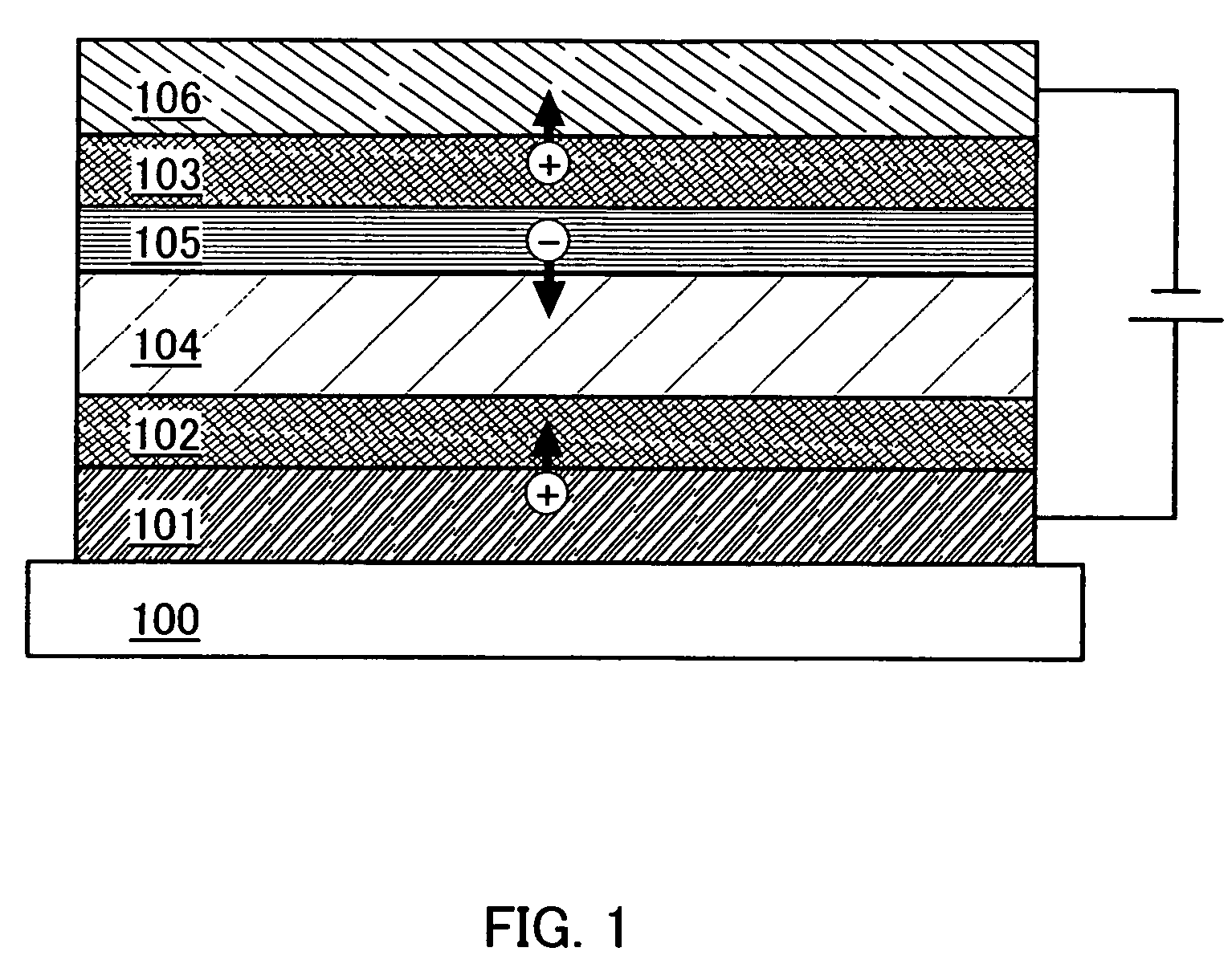
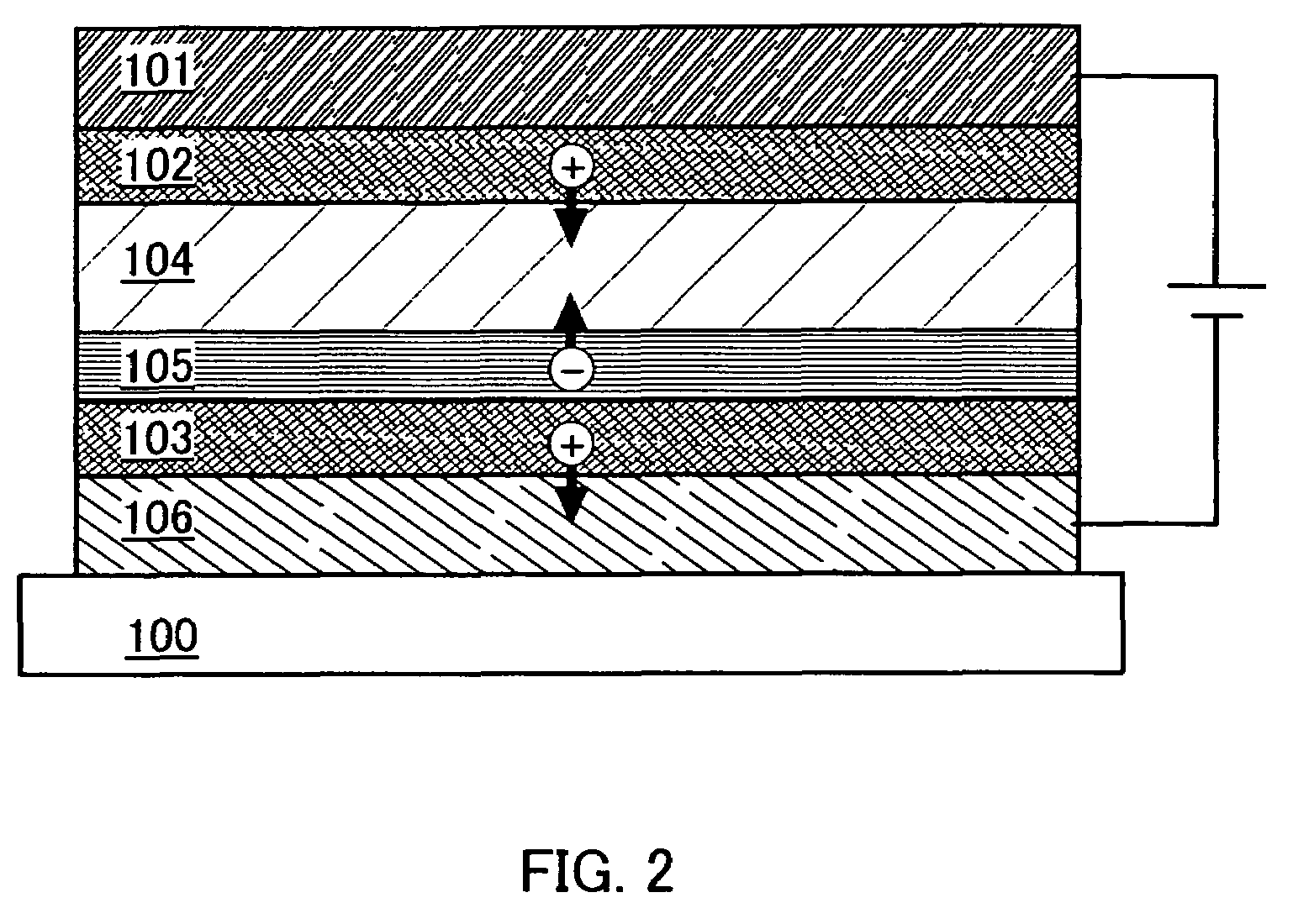
[0045]The present embodiment mode describes the structure of a light-emitting element of the present invention with reference to FIGS. 1 and 2. In a light-emitting element according to the present invention, a light-emitting layer 104 containing a light-emitting material and an electron-generating layer 105 are stacked, and the light-emitting layer 104 and the electron-generating layer 105 are sandwiched between a first hole-generating layer 102 and a second hole-generating layer 103. The first hole-generating layer 102 and the second hole-generating layer 103 are further sandwiched between an anode 101 and a cathode 106, and stacked over an insulator 100 such as a substrate or an insulating film. Over the insulator 100 such as the substrate or the insulating film, the anode 101, the first hole-generating layer 102, the light-emitting layer 104, the electron-generating layer 105, the second hole-generating layer 103, and the cathode 106 are stacked in order (FIG. 1). Alternatively, ...

embodiment mode 2

[0054]Another embodiment mode of the present invention is described. The present embodiment mode describes an example of improving the characteristic of a viewing angle of a light-emitting element and a display device by appropriately adjusting the thicknesses of the first hole-generating layer 102 and the second hole-generating layer 103. Since the multilayer structure and the material of the light-emitting element in the present embodiment mode are the same as those in Embodiment Mode 1, the description is omitted here. Refer to Embodiment Mode 1.

[0055]Light emitted from the light-emitting element include light directly emitted from the light-emitting layer 104 and light emitted after being reflected once or multiple times. The light directly emitted and the light emitted after being reflected interfere in accordance with the relation between their phases so that they are intensified or attenuated with each other. Therefore, the light emitted from the light-emitting element is lig...

embodiment mode 3

[0071]This embodiment mode describes a display device according to the present invention shown in Embodiment Mode 1 or Embodiment Mode 2 while showing its manufacturing method with reference to FIGS. 5A to 6C. Although this embodiment mode shows an example of manufacturing an active matrix display device, a light-emitting element of the present invention is also applicable for a passive matrix display device.

[0072]First, a first base insulating layer 51a and a second base insulating layer 51b are formed over a substrate 50, and then a semiconductor layer is formed over the second base insulating layer 51b (FIG. 5A).

[0073]As a material of the substrate 50, glass, quartz, plastic (such as polyimide, acrylic, polyethylene terephthalate, polycarbonate, polyacrylate, or polyethersulfone), or the like can be used. These substrates may be used after being polished by CMP or the like as necessary. In this embodiment mode, a glass substrate is used.

[0074]The first base insulating layer 51a a...


PUM


Abstract

The present invention provides a light-emitting element having a structure in which the drive voltage is comparatively low and a light-emitting element in which the increase in the drive voltage over time is small. Further, the present invention provides a display device in which the drive voltage and the increase in the drive voltage over time are small and which can resist long-term use. A layer in contact with an electrode in a light-emitting element is a layer containing a P-type semiconductor or a hole-generating layer such as an organic compound layer containing a material having electron-accepting properties. The light-emitting layer is sandwiched between the hole-generating layers, and an electron-generating layer is sandwiched between the light-emitting layer and the hole-generating layer on a cathode side.

Description

BACKGROUND OF THE INVENTION[0001]1. Field of the Invention[0002]The present invention relates to a light-emitting element which sandwiches a thin film containing a light-emitting material between electrodes and which emits light by applying current. Moreover, the present invention relates to a display device and an electronic appliance which use the light-emitting element.[0003]2. Related Art[0004]A display using a thin film light-emitting element of a self-light-emitting type, which emits light by itself when current is applied, has been extensively developed.[0005]This thin film light-emitting element emits light by connecting an electrode to a single-layer or multilayer thin film formed using one or both of organic compound and inorganic compound and by applying current. Such a thin film light-emitting element is expected to reduce the power consumption, occupy smaller space, and increase the visibility, and the market is also expected to expand further.[0006]It has become possib...

Claims


Application Information

Patent Timeline
Patent Type & Authority Patents(United States)
IPC IPC(8): H01L27/15H01L51/50
CPCH01L51/5052H01L51/5048H01L27/3244H01L2251/558H10K59/12H10K50/157H10K50/155H10K50/165H10K50/15H10K50/16H10K2102/351H05B33/02
Inventor KUMAKI, DAISUKESEO, SATOSHI
Owner SEMICON ENERGY LAB CO LTD
Why Eureka
Try Eureka