BiCMOS performance enhancement by mechanical uniaxial strain and methods of manufacture

a technology of mechanical uniaxial strain and bicmos, which is applied in the direction of semiconductor devices, semiconductor/solid-state device details, electrical apparatus, etc., can solve the problems of biaxial compressive strain actually having a detrimental effect on the performance of other cmoss on the same chip, work to degrade the performance of nmos or bjt, and uniaxial tensile strain in the direction of collector curren

Active Publication Date: 2008-12-16
TAIWAN SEMICON MFG CO LTD
View PDF8 Cites 36 Cited by
  • Summary
  • Abstract
  • Description
  • Claims
  • Application Information

AI Technical Summary

Benefits of technology

[0011]These aspects of the present invention allow for each device to be separately enhanced by the dielectric films. This allows for an enhancement of each device without the usual degradation of performance of the other devices on the same chip.

Problems solved by technology

This inevitably results in a biaxial compressive strain, which causes a uniaxial tensile strain in the direction of collector current.
However, while this biaxial compressive strain has been reported to enhance Bipolar Junction Transistors (BJTs) and Heterojunction Bipolar Transistors (HBTs), the biaxial compressive strain actually has a detrimental effect on the performance of other CMOSs on the same chip, especially for an NMOS transistor.
However, the same compressive CESL, if formed over either an NMOS transistor or a BJT, will actually work to degrade the performance of the NMOS or BJT.
Unfortunately, this tensile CESL will have the opposite effect upon a PMOS transistor on the same chip, and will degrade the performance of the PMOS transistor.

Method used


Image

  • BiCMOS performance enhancement by mechanical uniaxial strain and methods of manufacture
  • BiCMOS performance enhancement by mechanical uniaxial strain and methods of manufacture
  • BiCMOS performance enhancement by mechanical uniaxial strain and methods of manufacture

Examples


Embodiment Construction

[0021]The making and using of the presently preferred embodiments are discussed in detail below. It should be appreciated, however, that the present invention provides many applicable inventive concepts that can be embodied in a wide variety of specific contexts. The specific embodiments discussed are merely illustrative of specific ways to make and use the invention, and do not limit the scope of the invention.

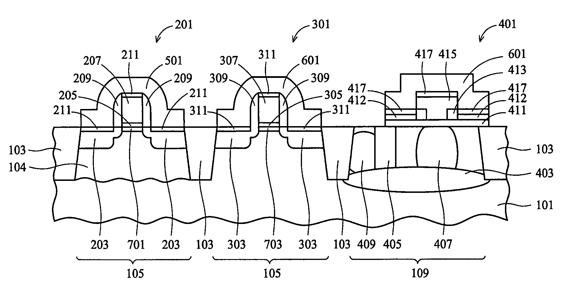
[0022]The present invention will be described with respect to steps in manufacturing the preferred embodiments in a specific context, namely a BiCMOS with a PMOS transistor, an NMOS transistor, and a BJT, where a tensile CESL is located on the NMOS transistor and a compressive CESL is located on the PMOS transistor and the BJT. The invention may also be applied in the making of other semiconductor devices.

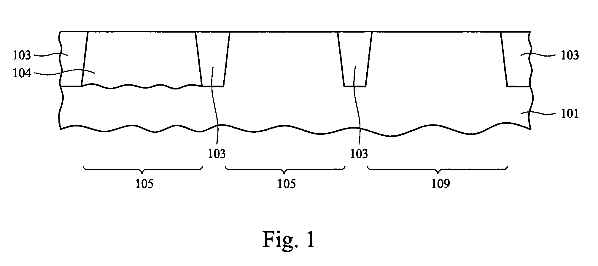
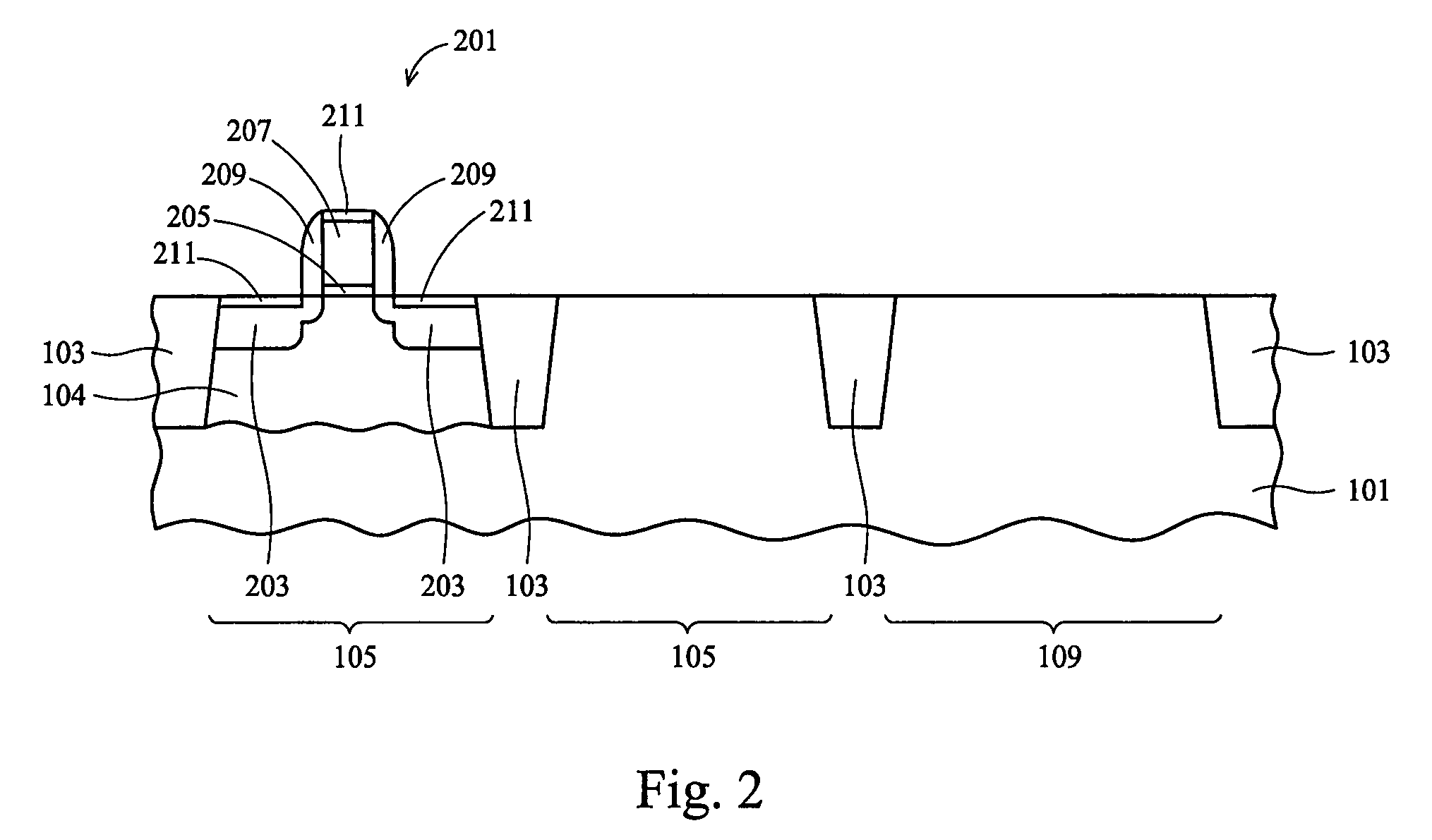
[0023]FIG. 1 illustrates a substrate 101 with isolations regions 103 formed therein. The substrate 101 may comprise bulk silicon, doped or undoped, or an active layer of a s...


PUM


Abstract

A BiCMOS device with enhanced performance by mechanical uniaxial strain is provided. A first embodiment of the present invention includes an NMOS transistor, a PMOS transistor, and a bipolar transistor formed on different areas of the substrate. A first contact etch stop layer with tensile stress is formed over the NMOS transistor, and a second contact etch stop layer with compressive stress is formed over the PMOS transistor and the bipolar transistor, allowing for an enhancement of each device. Another embodiment has, in addition to the stressed contact etch stop layers, strained channel regions in the PMOS transistor and the NMOS transistor, and a strained base in the BJT.

Description

TECHNICAL FIELD[0001]The present invention relates generally to semiconductor devices, and more specifically to BiCMOS devices, and even more specifically to BiCMOS devices having multiple regions with different stresses.BACKGROUND[0002]Bipolar Complementary Metal Oxide Semiconductors (BiCMOS) devices are semiconductor devices that combine bipolar and Complementary Metal Oxide Semiconductors (CMOS) on the same chip. Increasing the performance of these BiCMOS devices has been a constant effort so as to maximize the efficiency and reduce the size of the BiCMOS device.[0003]Various methods have been used to increase the performance of BiCMOS devices. One such method involves forming a BiCMOS device with shallow trenches filled with a dielectric layer that has a lower thermal expansion coefficient than that of silicon. This inevitably results in a biaxial compressive strain, which causes a uniaxial tensile strain in the direction of collector current. However, while this biaxial compres...

Claims


Application Information

Patent Timeline
Patent Type & Authority Patents(United States)
IPC IPC(8): H01L27/06H01L27/07
CPCH01L21/823807H01L21/8249H01L27/0623H01L29/7843
Inventor KO, CHIH-HSINWANG, TZU-JUEICHEN, HUNG-WEIKE, CHUNG-HULEE, WEN-CHIN
Owner TAIWAN SEMICON MFG CO LTD
Why Eureka
Try Eureka