Coating for performance enhancement of semiconductor apparatus

a technology for semiconductor apparatus and coating, applied in the field of coating for performance enhancement of semiconductor apparatus, can solve the problems of affecting the corrosion of the plasma to the various elements of the chamber, so as to enhance the surface roughness of the coating, improve the performance of the coating packaged showerhead, and enhance the surface density and stability of the coating

Inactive Publication Date: 2014-05-01
ADVANCED MICRO FAB EQUIP INC CHINA
View PDF10 Cites 90 Cited by
  • Summary
  • Abstract
  • Description
  • Claims
  • Application Information

AI Technical Summary

Benefits of technology

[0023]In another embodiment, in order further to improve the performance of the coating packaged showerhead, surface processes are applied on the as-coated showerhead, which includes, but not limited to, surface smoothening or roughening to reduce the particles, surface modification to enhance the surface density and stability of the coatings, and surface chemical cleaning to remove the particles and contamination that are formed on the coated showerhead either due to the coating deposition process or due to the plasma etching process.
[0024]According to one aspect, the surface roughness of the A-coating is controlled, since if the surface is too smooth, polymer deposition during etching will not adhere well to the surface, and thus induce particles. On the other hand, too rough surface will directly create particles due to the plasma etching. The recommended surface roughness is at least 1 um or above for the A-coatings, which can be reached by the adjustment of the substrate roughness, by the deposition process, or by lapping, polishing and other post surface treatment on the deposited coatings.
[0025]According to another aspect, the energetic ion bombardment or plasma etching in the PEPVD is used to smooth/rough and densify the surface of A-coating coated showerhead. The coated showerhead surface can be cleaned by wet solution cleaning in which the erosive solution or slurry or aerosol is used to blast away the surface particles and to control the surface roughness of the coating either on the flat plate or inside the gas holes. The dense coating with the specified roughness could have the fine and compact grain structure with reduced porous volume defects, and thus reduce the plasma erosion rate and maintain clean environment during the plasma etch processes.
[0026]To reach performance improved etch processes, the coated showerhead can be formed with modification or combination of the gas distribution plate, showerhead aluminum base and the upper ground ring into one piece of coated showerhead, or the one piece of showerhead with the build-in heater, so that the formation of the new coated showerhead can reduce the production cost and the coated showerh

Problems solved by technology

This phenomenon is especially troublesome for showerheads having a chemical vapor deposited silicon carbide coating (CVD SiC).
As is known, during processing the plasma may be rather corrosive to the various elements of the chamber, especially the showerhead, since it forms a part of the capacitive RF power circuit.
Yttria (Y2O3) coating is believed to be promising; however, it has been very difficult to find a process that results in good coating, especially one that does not crack or generate particles.
However, conventional PS Y2O3 coating is formed by the sprayed Y2O3 particles, and generally results in a coating having high surface roughness (Ra of 4 micron or more) and relatively high porosity (volume fraction is above 3%).
The high surface roughness and porous structure makes the coating susceptible to generation of particles, which may contaminate the wafer being processed.
In addition, the particle will come out from the gas holes and dropped on the wafer when the as-coated shower head is used in the plasma process, as the plasma sprayed coatin

Method used


Image

  • Coating for performance enhancement of semiconductor apparatus
  • Coating for performance enhancement of semiconductor apparatus
  • Coating for performance enhancement of semiconductor apparatus

Examples


Embodiment Construction

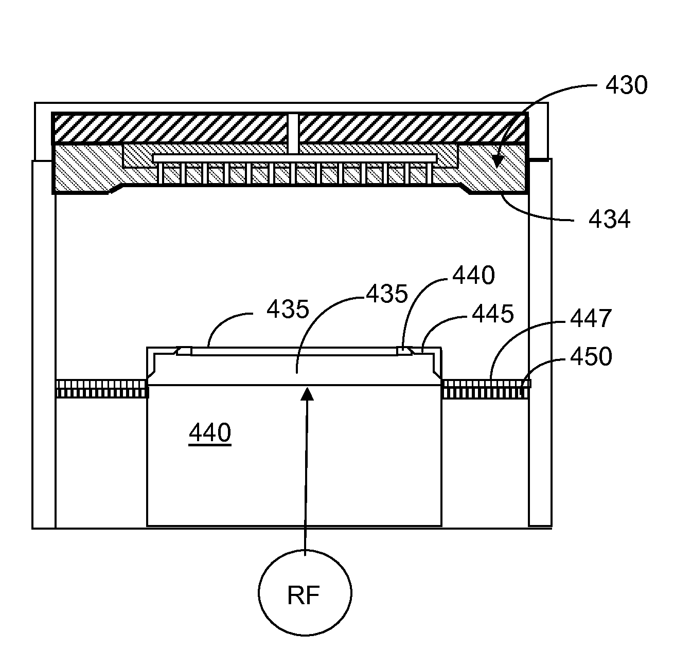
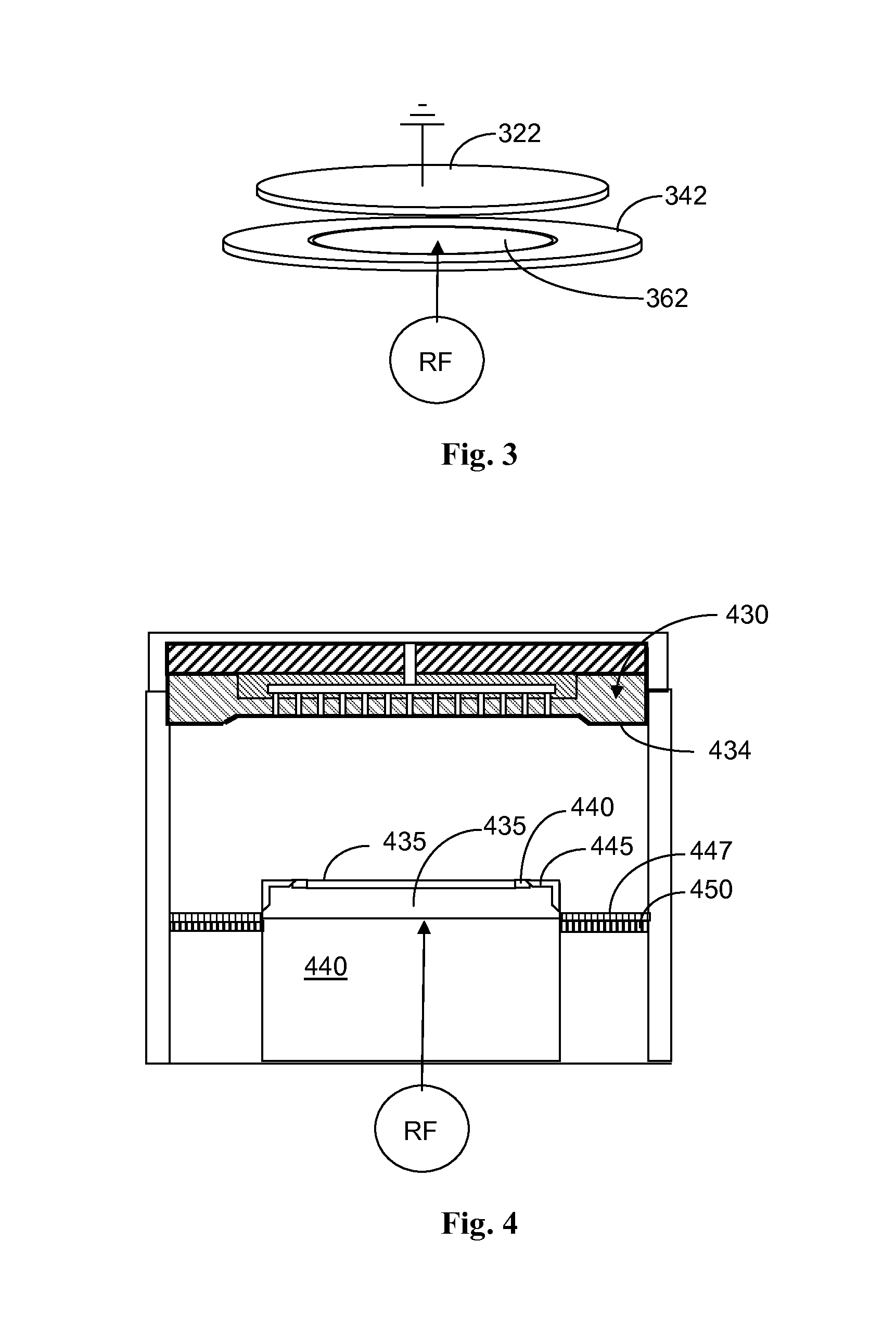
[0044]Various embodiments will now be described, providing improved coatings for showerheads, which improve erosion and particle performance of the showerhead, together with coated cathode assembly for enhancing etch rate and plasma uniformity. FIG. 3 is a schematic illustrating the arrangement for a capacitively coupled plasma chamber. In this embodiment, the top electrode 322 is grounded and the RF power is applied to the bottom electrode, which in this example is composed of electrode 362 and extension 342. The top electrode 322 may be composed of the perforated plate, or a combination of perforated plate and grounding ring. The bottom electrode 362 may be embedded in the chuck, or be part of the pedestal supporting the chuck. The extension 342 may be composed of one or a combination of focus ring, cover ring, flow equivalent ion shied, and / or plasma confinement ring. By proper selection of the elements comprising the upper and lower electrodes, and proper coating of these elemen...


PUM

PropertyMeasurementUnit
Porosityaaaaaaaaaa
Surface roughnessaaaaaaaaaa

Abstract

A plasma processing chamber having advanced coating for the showerhead and for an extended bottom electrode. The extended bottom electrode can be formed by one or more of the focus ring, cover ring, and plasma confinement ring. The extended electrode can be formed using a one-piece composite cover ring. The composite cover ring may be made of Al2O3 and include a Y2O3 plasma resistant coating. The plasma confinement ring may include a flow equalization ion shield that may also be provided with the plasma resistant coating. The plasma resistant coating of the extended electrode may have elements matching that of the showerhead.

Description

[0001]This application claims the priority of Chinese Patent Application No. 201210421964.4, entitled “COATING FOR PERFORMANCE ENHANCEMENT OF SEMICONDUCTOR APPARATUS”, filed with the Chinese Patent Office on Oct. 29, 2012, which is incorporated by reference in its entirety herein.BACKGROUND[0002]1. Field[0003]The subject invention relates to plasma processing chambers and, in particular, to chamber arrangements using coating for internal chamber parts, which enhance the performance of the plasma chamber.[0004]2. Related Art[0005]In plasma processing chambers, a showerhead is often used to inject the process gas. In certain plasma chambers, such as capacitively-coupled plasma chambers, the showerhead may also function as an electrode, coupled to either ground or RF potential. However, during processing the showerhead is exposed to the plasma and is attacked by the active species within the plasma, such as halogen plasma of CF4, Cl2, etc. This phenomenon is especially troublesome for ...

Claims


Application Information

Patent Timeline
IPC IPC(8): C23C16/44
CPCC23C16/4404C23C14/028C23C14/0694C23C14/083C23C14/32C23C14/5873H01J37/32477H01J37/32495H01J37/32559H01J37/32623H01J37/32642Y10T29/49888C23C14/06C23C14/22C23C14/34
Inventor HE, XIAOMINGZHANG, LICHEN, XINGJIANNI, TUQIANGXU, ZHAOYANG
Owner ADVANCED MICRO FAB EQUIP INC CHINA
Why Eureka
Try Eureka