Selection method of bit line redundancy repair and apparatus performing the same
- Summary
- Abstract
- Description
- Claims
- Application Information
AI Technical Summary
Benefits of technology
Problems solved by technology
Method used
Image


Examples
first embodiment
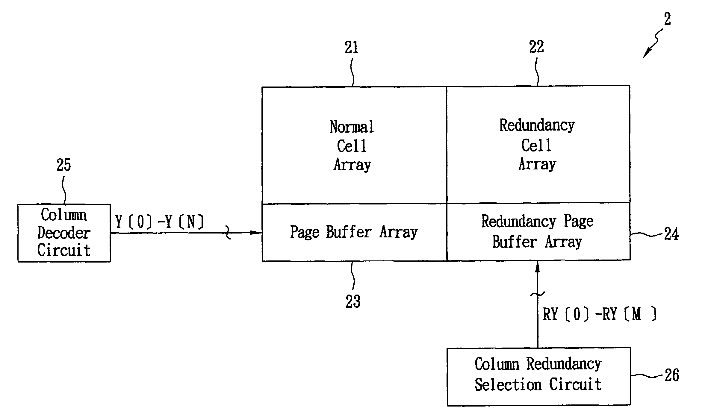
[0036]FIG. 6 shows the column redundancy selection circuit 26, which is applied to the semiconductor memory device 2 in FIG. 5(b), according to the present invention. The column redundancy selection circuit 26 includes a redundancy repair enable circuit 261 generating a redundancy enable signal RED based on logical addresses ADD1 of the memory blocks, a controlling fuse circuit 262 sending a code matching a defective type of the memory blocks, and a redundancy decoder circuit 263 receiving the redundancy enable signal RED, logical addresses ADD2 of the memory blocks and the code to generate a plurality of redundancy selection signals RY selecting a plurality of redundancy blocks in the redundancy cell array 22 to replace a plurality of memory blocks in the normal cell array 21. In the current embodiment, the redundancy repair enable circuit 261 includes a redundancy enable circuit 261a (refer to FIG. 7(a)), an enable fuse circuit 261b (refer to FIG. 7(b)), and three fuse state circu...
second embodiment
[0041]For the column redundancy selection circuit 26′ in FIG. 6, which is applied to the semiconductor memory device 2′ in FIG. 5(c), according to the present invention, the redundancy repair enable circuit 261′ includes a redundancy enable circuit 261a′ (refer to FIG. 10), an enable fuse circuit 261b′ (refer to FIG. 7(b)), and three fuse state circuits 261c′ (refer to FIG. 7(c)). The redundancy enable circuit 261a′ receives the enable fuse signal EN, the fuse state signals FA[2]-FA[4], an extra fuse signal FS[3] and three bits A[2]-A[4] of the logical addresses (indicated as ADD1 in FIG. 6) of the memory blocks. Similarly to FIG. 7(a), when the bit A[2] is equal to the fuse state signal FA[2], the bit A[3] is equal to the fuse state signal FA[3], and the bit A[4] is equal to the fuse state signal FA[4], respectively, the gates EQ6, EQ8 and EQ9 will output logic 1. However, in contrast to FIG. 7(a), FS[3] is added to initiate one input of the gate NA15 even if the gate EQ6 outputs l...
PUM
 Abstract
Description
Claims
Application Information