

Semiconductor memory device for storing multilevel data
a memory device and semiconductor technology, applied in the field of semiconductor memory devices capable of storing multi-level data, can solve the problems of increasing the threshold voltage of the cell in which data has already been written, and the inability to complete the writing of data into the preceding cell
- Summary
- Abstract
- Description
- Claims
- Application Information
AI Technical Summary
Benefits of technology
Problems solved by technology
Method used
Image

Examples
first embodiment
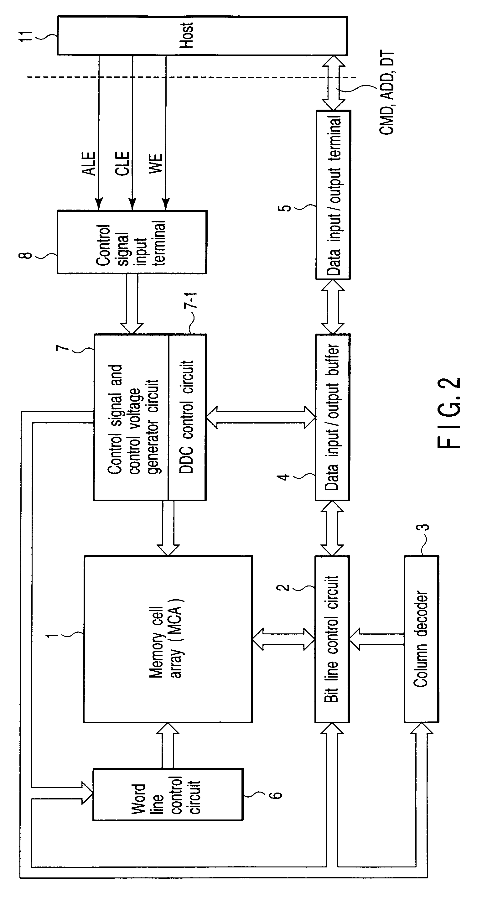
[0050]FIG. 2 shows a schematic configuration of a NAND flash memory which stores, for example, 3-bit, 8-level data.
[0051]A memory cell array 1 includes a plurality of bit lines, a plurality of word lines, and a common source line. In the memory cell array 1, electrically rewritable memory cells made up of, for example, EEPROM cells are arranged in a matrix. A bit line control circuit 2 for controlling bit lines and a word line control circuit 6 are connected to the memory cell array 1.
[0052]The bit line control circuit 2 reads the data in a memory cell of the memory cell array 1 via a bit line, detects the state of a memory cell of the memory cell array 1 via a bit line, and writes data into a memory cell of the memory cell array 1 by applying a write control voltage to the memory cell via a bit line. A column decoder 3 and a data input / output buffer 4 are connected to the bit line control circuit 2. A data storage circuit in the bit line control circuit 2 is selected by the column ...
second embodiment
[0113]FIG. 16 shows a second embodiment of the invention. The same parts as those in FIG. 1 are indicated by the same reference numerals. In the second embodiment, the host 11 outputs a specific command, for example, a command to lower the write speed, following the last data supplied to the NAND flash memory, and the control signal and control voltage generator circuit 7 decreases, for example, the write speed according to the command.
[0114]For example, in the write sequence shown in FIG. 15, the same write operation as described above is carried out according to steps S11, S2, S3, S4, and S5 shown in FIG. 16 until the host 11 outputs a specific command.
[0115]On the other hand, for example, if the page addresses 3, 4, 5 are the last ones, control is passed from step S11 to step S12. In this case, the host 11 outputs a specific command following the page addresses 3, 4, 5. Receiving the command (S12), the control signal and control voltage generator circuit 7 lowers, for example, th...
third embodiment
[0119]FIG. 17 shows a third embodiment of the invention. The same parts as those in FIG. 1 are indicated by the same reference numerals.
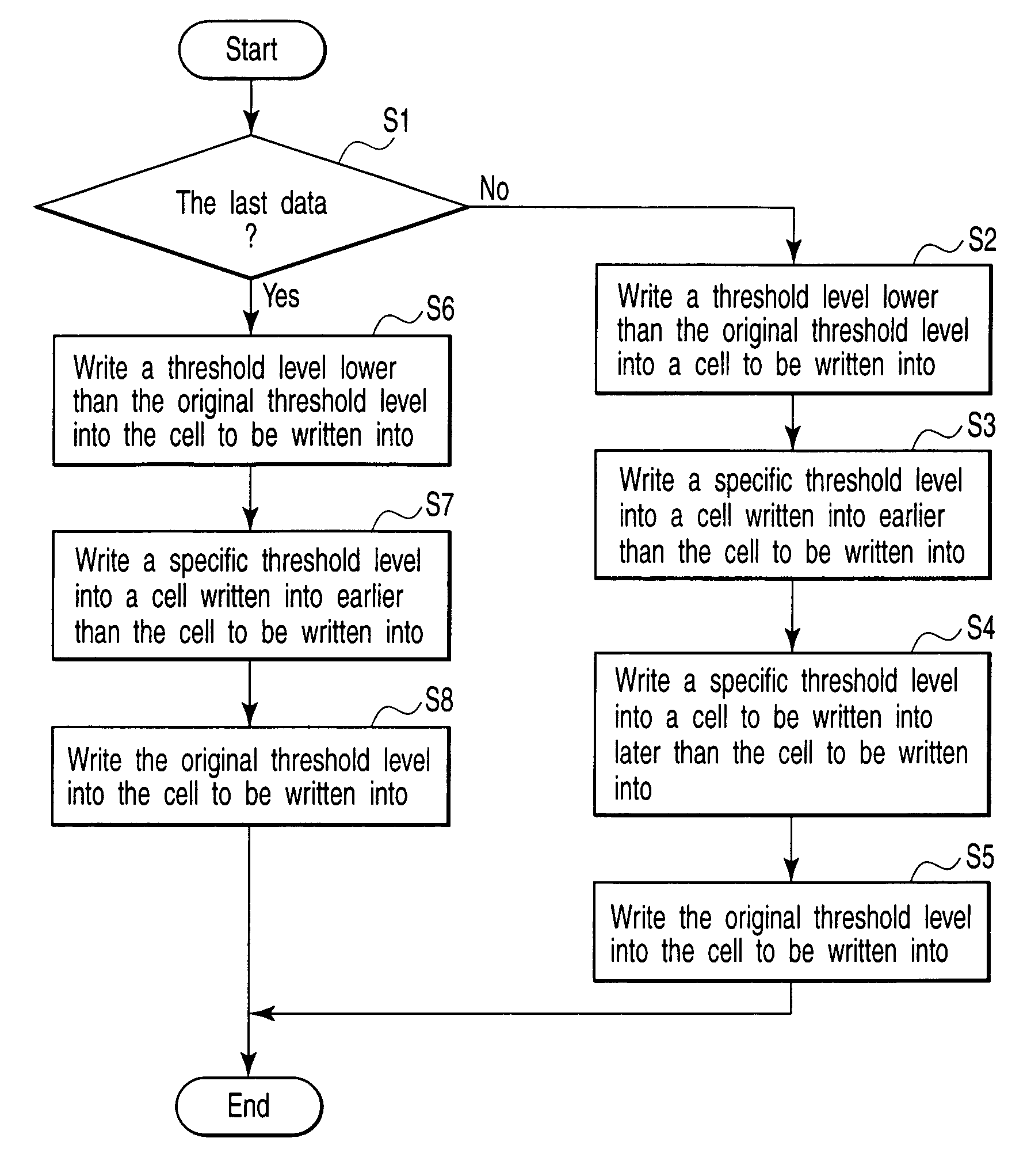
[0120]For example, in the write sequence shown in FIG. 15, the operation excluding the beginning and end of the write operation is the same as in the first embodiment. In FIG. 15, for example, if the page addresses 3, 4, 5 in writing [1] is for the last writing, that is, if the host 11 has not sent data for writing [3], control is passed from step S1 to step S22, where a lower threshold level than the original threshold level is written into the cell to be written into as shown in FIGS. 14A and 14B.
[0121]Thereafter, when writing is started again and the host 11 supplies a write command together with the write data for adjacent cells, control is passed from step S21 to step S23. In step S23, for example, the host 11 supplies the data in the page addresses 6, 7, 8 shown in writing [3] for the preceding writing [1], the data in the cell written into at...
PUM
 Abstract
Description
Claims
Application Information