Method for making a self-converged void and bottom electrode for memory cell

a memory cell and bottom electrode technology, applied in the manufacturing of basic electric elements, semiconductor/solid-state devices, electric devices, etc., can solve the problems of high density memory devices, lack of uniformity or reliability needed for large-scale use, and limited cell manufacturing processes of standard integrated circuit manufacturing processes

Active Publication Date: 2009-01-06
MACRONIX INT CO LTD
View PDF234 Cites 96 Cited by
  • Summary
  • Abstract
  • Description
  • Claims
  • Application Information

AI Technical Summary

Problems solved by technology

One problem associated with phase change memory devices arises because the magnitude of the current required for reset operations depends on the volume of phase change material that must change phase.
Thus, cells made using standard integrated circuit manufacturing processes have been limited by the minimum feature size of manufacturing equipment.
Thus, techniques to provide sublithographic dimensions for the memory cells must be developed, which can lack uniformity or reliability needed for large scale, high density memory devices.

Method used


Image

  • Method for making a self-converged void and bottom electrode for memory cell
  • Method for making a self-converged void and bottom electrode for memory cell
  • Method for making a self-converged void and bottom electrode for memory cell

Examples


Embodiment Construction

[0026]The following description of the invention will typically be with reference to specific structural embodiments and methods. It is to be understood that there is no intention to limit the invention to the specifically disclosed embodiments and methods but that the invention may be practiced using other features, elements, methods and embodiments. Preferred embodiments are described to illustrate the present invention, not to limit its scope, which is defined by the claims. Those of ordinary skill in the art will recognize a variety of equivalent variations on the description that follows. Like elements in various embodiments are commonly referred to with like reference numerals.

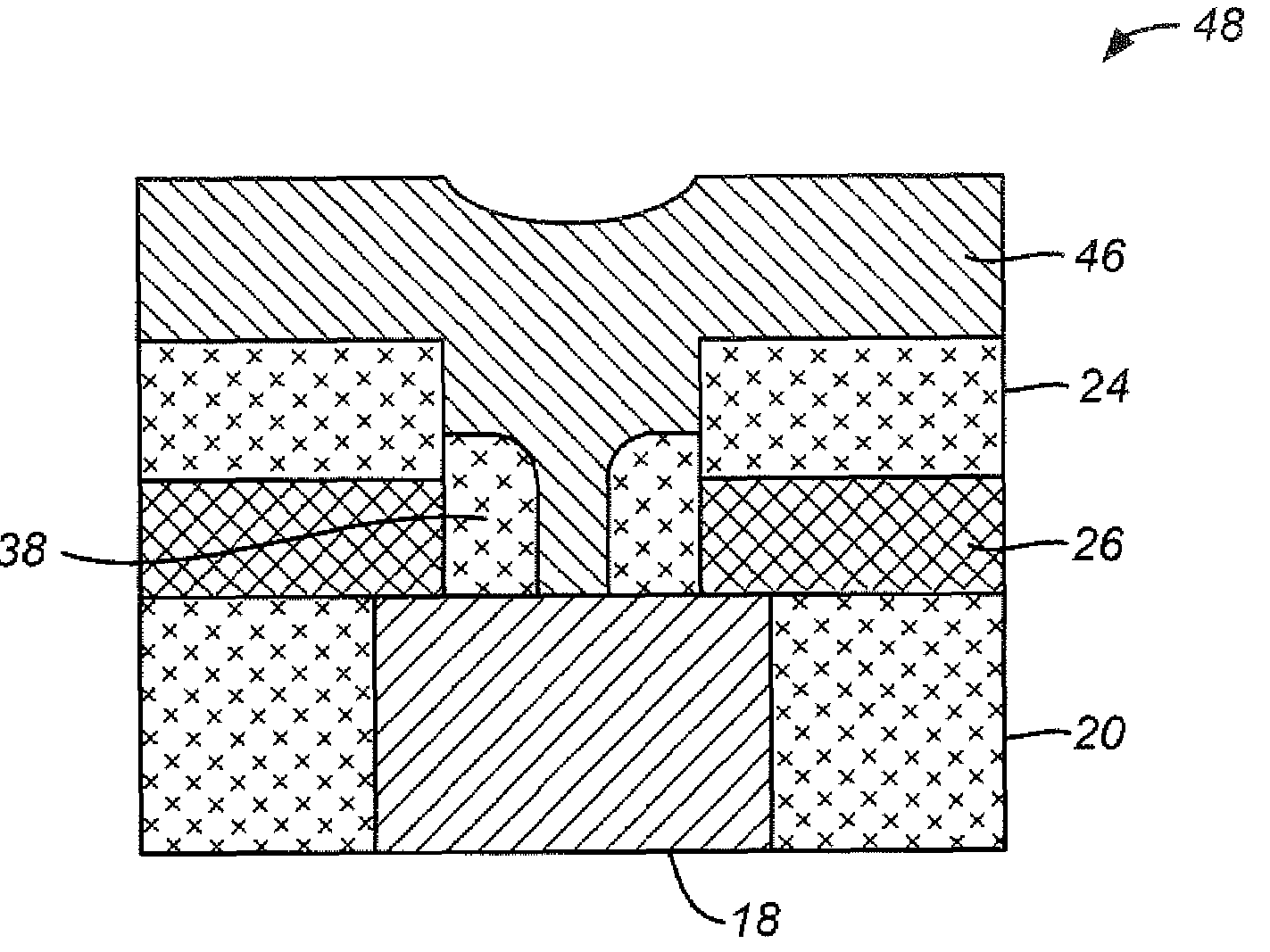
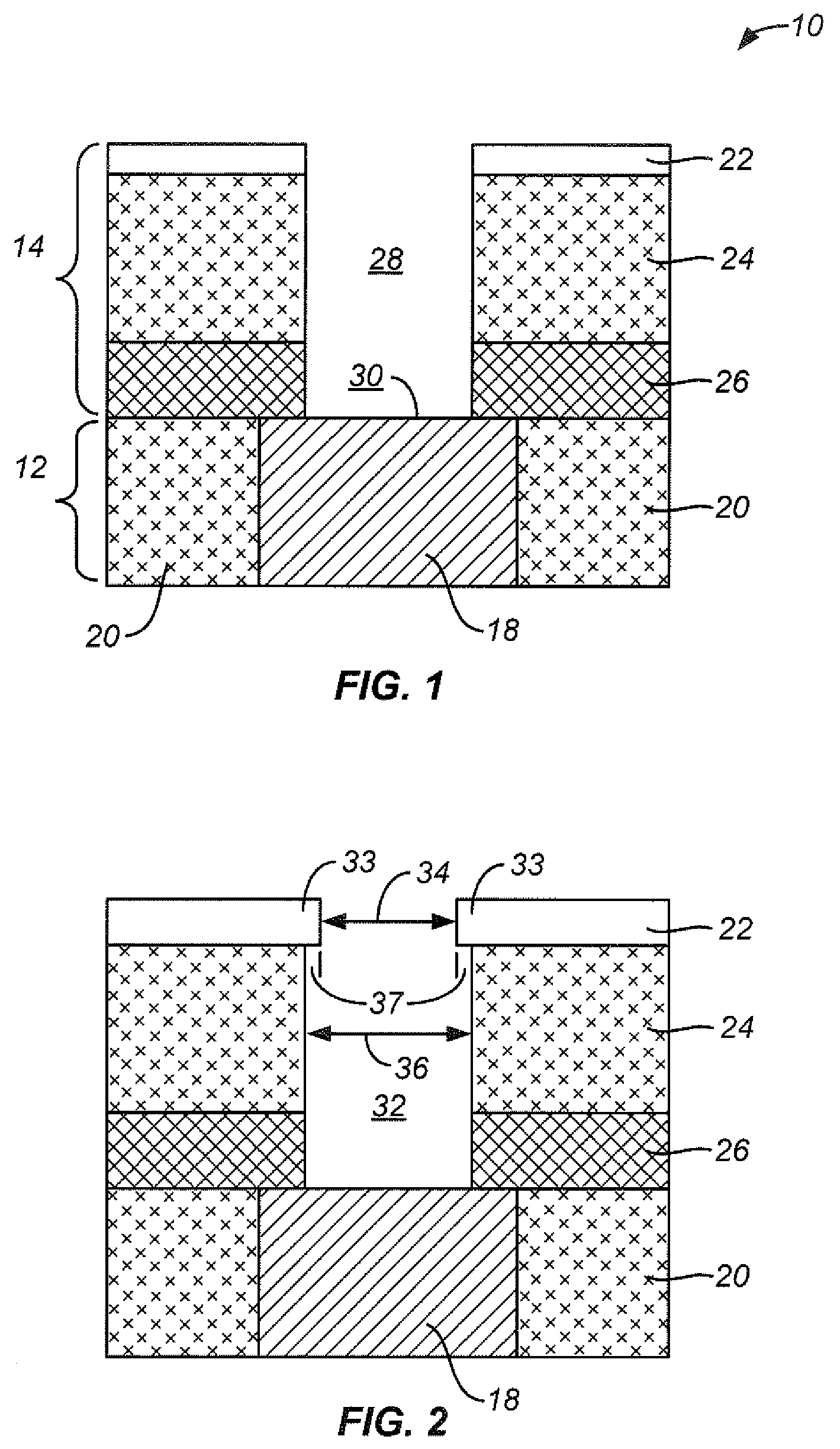
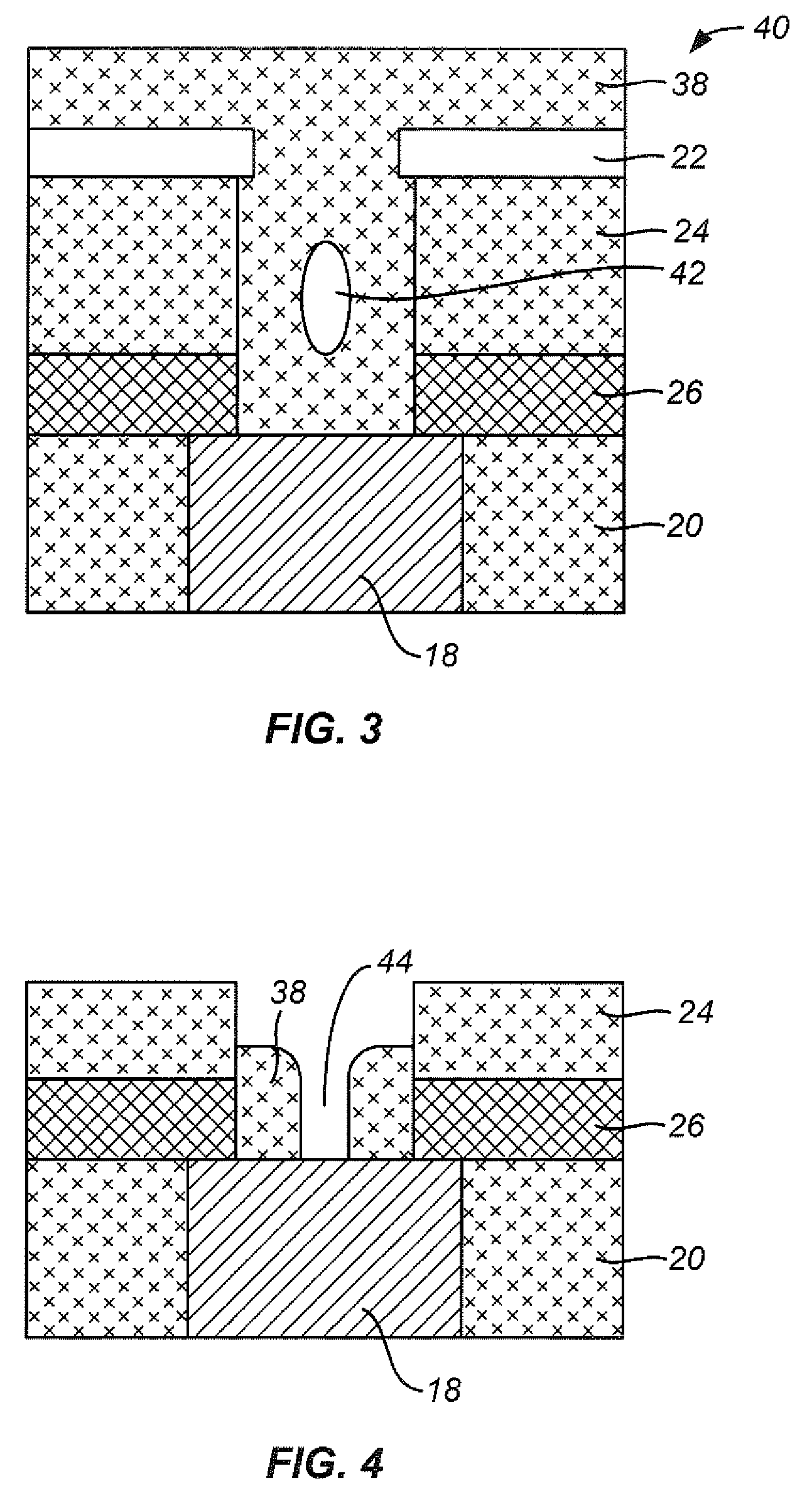
[0027]FIG. 1 is a simplified side view of a first memory cell subassembly 10 including a base layer 12 and an upper layer 14. Base layer 12 includes a plug 18, acting as electrically conductive element 18, within an oxide layer 20. Plug 18 is typically made of TiN or tungsten while oxide layer 20 is typi...


PUM


Abstract

A base layer, comprising an electrically conductive element, is formed. An upper layer, including a third, lower planarization stop layer, a second layer and a first, upper layer is formed on the base layer. A keyhole opening is formed through the upper layer to expose a surface of an electrically conductive element in the base layer. The first layer has an overhanging portion extending into the opening so that the opening in the first layer is shorter than in the second layer. A dielectric material is deposited into the keyhole opening to create a self-converged void within the deposited dielectric material. In some examples the keyhole forming step comprises increasing the volume of the first layer while in other examples the keyhole forming step comprises etching back the second layer.

Description

CROSS-REFERENCE TO OTHER APPLICATIONS[0001]This application is related to the following US patent applications, each filed on the same day as this application, assigned to the same assignee and having the same inventor: Method for Making a Self-Converged Memory Material Element for Memory Cell, Ser. No 11 / 567,300, and Method for Making a Keyhole Opening During the Manufacture of a Memory Cell, Ser. No. 11 / 567,314.PARTIES TO A JOINT RESEARCH AGREEMENT[0002]International Business Machines Corporation, a New York corporation; Macronix International Corporation, Ltd., a Taiwan corporation, and Infineon Technologies A.G., a German corporation, are parties to a Joint Research Agreement.BACKGROUND OF THE INVENTION[0003]1. Field of the Invention[0004]The present invention relates to high density memory devices based on memory materials, for example resistor random access memory (RRAM) devices, and to methods for manufacturing such devices. The memory material is switchable between electrica...

Claims


Application Information

Patent Timeline
Patent Type & Authority Patents(United States)
IPC IPC(8): H01L21/06
CPCH01L45/04H01L45/06H01L45/1233H01L45/1273H01L45/16H01L45/144H01L45/146H01L45/147H01L45/14H10N70/20H10N70/8418H10N70/881H10N70/8836H10N70/231H10N70/011H10N70/8828H10N70/8833H10N70/826
Inventor LUNG, HSIANG-LAN
Owner MACRONIX INT CO LTD
Why Eureka
Try Eureka