Method and apparatus that provides differential connections with improved ESD protection and routing

a technology of differential connection and esd protection, applied in the direction of circuit electrostatic discharge protection, overvoltage circuit protection, high frequency circuit adaptation, etc., can solve the problems of discontinuities in the impedance producing failures, non-uniform parasitic return path impedance, and adverse effect on signal integrity

Active Publication Date: 2009-01-20
SEMICON COMPONENTS IND LLC
View PDF4 Cites 8 Cited by
  • Summary
  • Abstract
  • Description
  • Claims
  • Application Information

AI Technical Summary

Benefits of technology

[0008]The present invention provides a single ESD device package that can be used to provide ESD protection to multiple high-speed lines, in particular multiple high-speed differential lines.
[0010]In another aspect of the invention, TMDS signal discontinuities are reduced by allowing uniform straight through routing. Such uniform straight through routing provides full ESD protection with improved impedance matching, which saves board space by integrating multiple functions.

Problems solved by technology

These considerations can be at odds with each other, since providing ESD protection requires some type device that will add a capacitance or inductance to the line, thereby having an adverse effect on signal integrity.
Adding any ESD device on top of these lines (i.e. capacitance and inductance) can cause discontinuities in the impedance producing a failure (according to the HDMI spec).
As a result, conventional interface devices that offer ESD protection for the HDMI and DVI specifications use multiple ESD protection chips or, as illustrated in FIGS. 1(a)-(c) route high speed lines in various circuitous paths, which then also lead to non-uniform parasitic return path impedance.
As such, there is a significant increase in impedance discontinuities and increase induced parasitics when routed normally.
Further, a greater area of board space is consumed.
As a result, greater signal skew exists at the receiver because of uncontrolled parasitics from the different ESD devices.

Method used


Image

  • Method and apparatus that provides differential connections with improved ESD protection and routing
  • Method and apparatus that provides differential connections with improved ESD protection and routing
  • Method and apparatus that provides differential connections with improved ESD protection and routing

Examples


Embodiment Construction

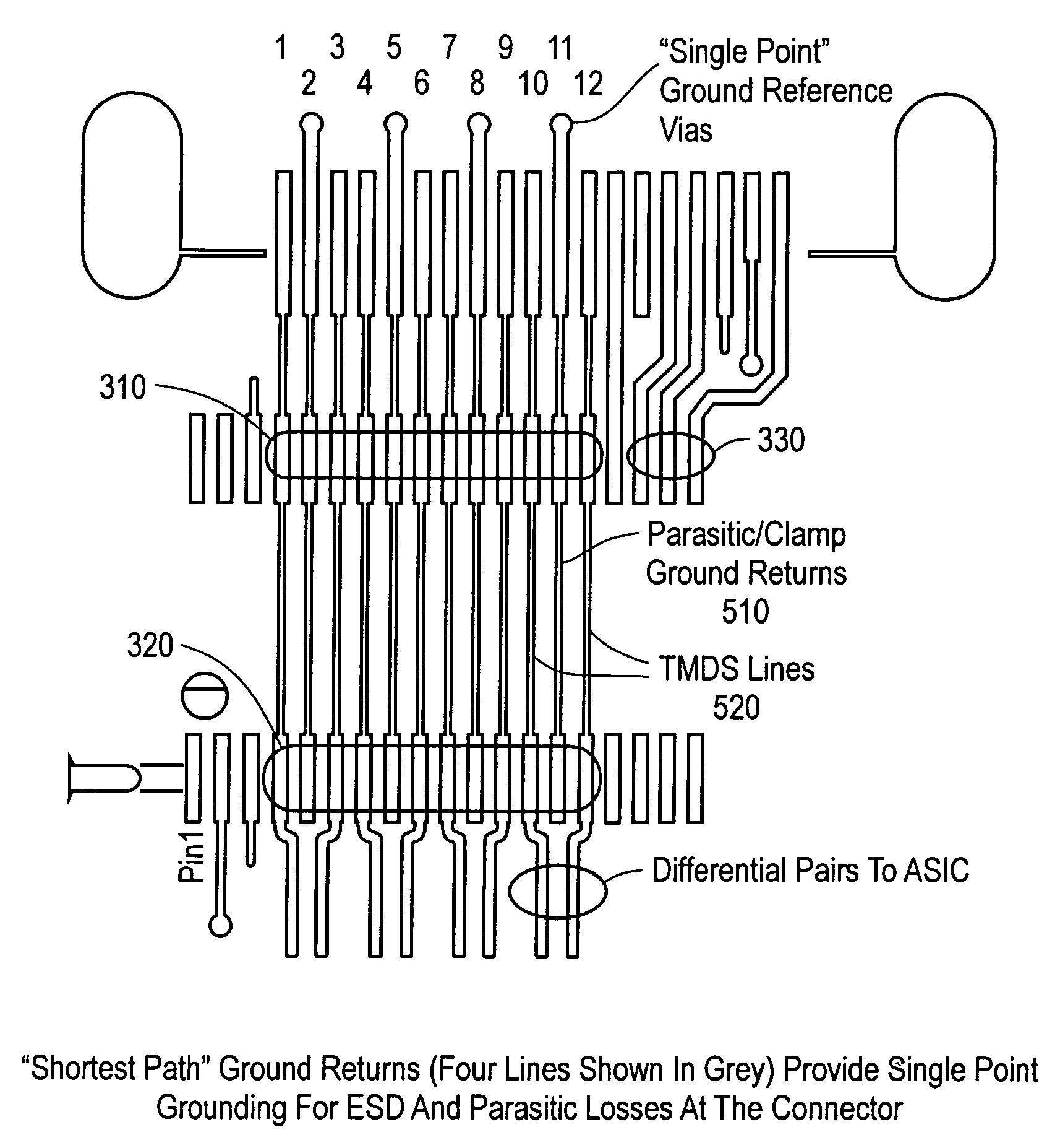
[0021]The present invention provides a single ESD device package that can be used to provide ESD protection to multiple high-speed lines, in particular multiple high-speed differential lines, such as TDMS lines of HDMI, or other lines subject to parasitics.

[0022]FIGS. 3(a) and 3(b) illustrates one aspect of the single ESD device package, which in this embodiment is for an HDMI interface that has four different differential TDMS lines. As illustrated in FIG. 3(a), the leadframe 302 contains symmetrical central leadframe pins 310 on one side of the leadframe 302, another set of symmetrical central leadframe pins 320 on the other side of the leadframe 302, and peripheral leadframe pins 330. It is noted that the pins 310 and 320 have relatively uniform internal dimensions as well as are straight, thus keeping the resultant parasitic TMDS lines skewed equally, as compared to bonding to the peripheral leadframe pins 330.

[0023]Area 340 of the leadframe will, as is known, have the die (not ...


PUM


Abstract

The present invention provides a single ESD device package that can be used to provide ESD protection to multiple high-speed lines, in particular multiple high-speed differential lines. The present invention has various aspects. Minute parasitic matching is achieved within a single package, and TMDS signal discontinuities are reduced by allowing uniform straight through routing. Also, the straight through routing and pin locations are matched to allow those straight routing lines to mate directly to high speed lines. Also, straight ground lines having a single via are associated with the straight through routing lines.

Description

BACKGROUND OF THE INVENTION[0001]1. Field of the Invention[0002]The present invention relates to a method and apparatus that provides differential connections with improved ESD protection and routing, and particularly a method and apparatus that provides differential connections which meet HDMI and DVI specifications.[0003]2. Background of the Related Art[0004]When routing high speed data signals between two points, it is well-known that many competing considerations exist in order to maintain the integrity of the signals.[0005]For certain high speed lines, there is desired to maintain both integrity of the signal, as well as obtain electrostatic discharge (ESD) protection. These considerations can be at odds with each other, since providing ESD protection requires some type device that will add a capacitance or inductance to the line, thereby having an adverse effect on signal integrity.[0006]In particular, HDMI has 4 pairs of differential, high speed data lines (TMDS lines) that m...

Claims


Application Information

Patent Timeline
Patent Type & Authority Patents(United States)
IPC IPC(8): H01L23/62
CPCH01L23/49541H01L23/50H01L24/05H01L23/60H01L23/66H01L2224/04042H01L2224/05553H01L2924/01033H01L2924/01006H01L2924/00014H01L24/48H01L2224/05599H01L2224/48247H01L2224/85399H01L2924/01005H01L2924/01082H01L2924/14H01L2924/30105H01L2924/30107H01L2924/3011H05K1/0237H05K1/0259H05K1/181H05K2201/09236H05K2201/10189H05K2201/10689H01L2224/45099H01L2924/00H01L24/49H01L2224/05554H01L2224/49171
Inventor DUNNIHOO, JEFFREY CMARAK, CHADWICK N.EVANS, MICHAEL S.
Owner SEMICON COMPONENTS IND LLC
Why Eureka
Try Eureka