Semiconductor device having align mark layer and method of fabricating the same

a technology of semiconductor devices and mark layers, which is applied in the direction of semiconductor devices, semiconductor/solid-state device details, electrical devices, etc., can solve the problems of alignment errors, alignment errors, and alignment apparatuses that may not achieve proper alignment for semiconductor devices, so as to reduce alignment errors

Active Publication Date: 2009-01-27
SAMSUNG ELECTRONICS CO LTD
View PDF11 Cites 21 Cited by
  • Summary
  • Abstract
  • Description
  • Claims
  • Application Information

AI Technical Summary

Benefits of technology

[0012]Exemplary embodiments of the present invention provide a semiconductor device having reduced alignment error.
[0013]In addition, exemplary embodiments of the present invention also provide a method of fabricating a semiconductor device that reduces alignment error during assembly of the semiconductor device and that is also cost-effective.

Problems solved by technology

However, a conventional alignment mark structure for a semiconductor device may cause alignment errors when the processes change during a fabricating operation.
However, a thickness (h) deviation of the passivation layer 60 formed on the align mark layer 55 may change the color of the portion of the align mark layer 55, and this color change may result in an alignment error for these semiconductor devices.
As optical alignment apparatus processes the alignment of a semiconductor device based upon the contrast between the field region and the align mark layer 55 within a standard range, these alignment apparatuses may as a result not achieve proper alignment for a semiconductor device having a contrast outside of the standard range.
Thus, it may be difficult to control the contrast by controlling the thickness (h) of the passivation layer 60.
Accordingly, even though the passivation layer 60 may be within an allowable process margin range, an alignment error with respect to the semiconductor device may still occur.

Method used


Image

  • Semiconductor device having align mark layer and method of fabricating the same
  • Semiconductor device having align mark layer and method of fabricating the same
  • Semiconductor device having align mark layer and method of fabricating the same

Examples


Embodiment Construction

[0025]The present invention will now be described more fully hereinafter with reference to the accompanying drawings, in which preferred embodiments of the invention are shown. This invention may, however, be embodied in many different forms and should not be construed as being limited to the embodiments set forth herein.

[0026]Structure

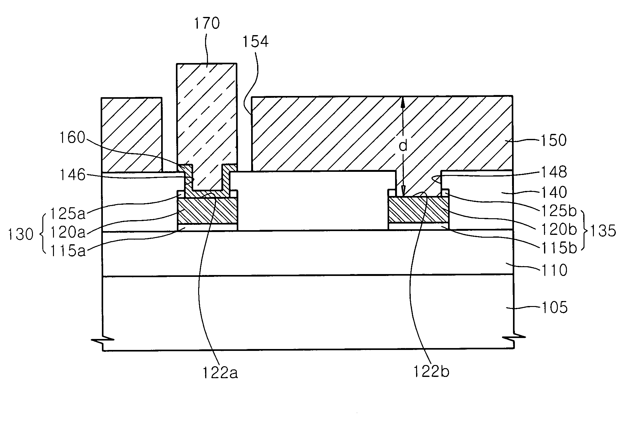
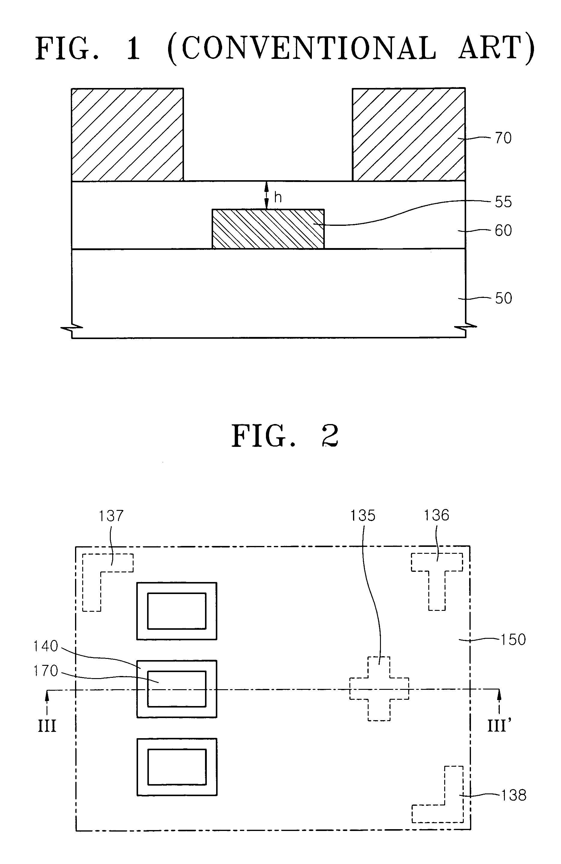
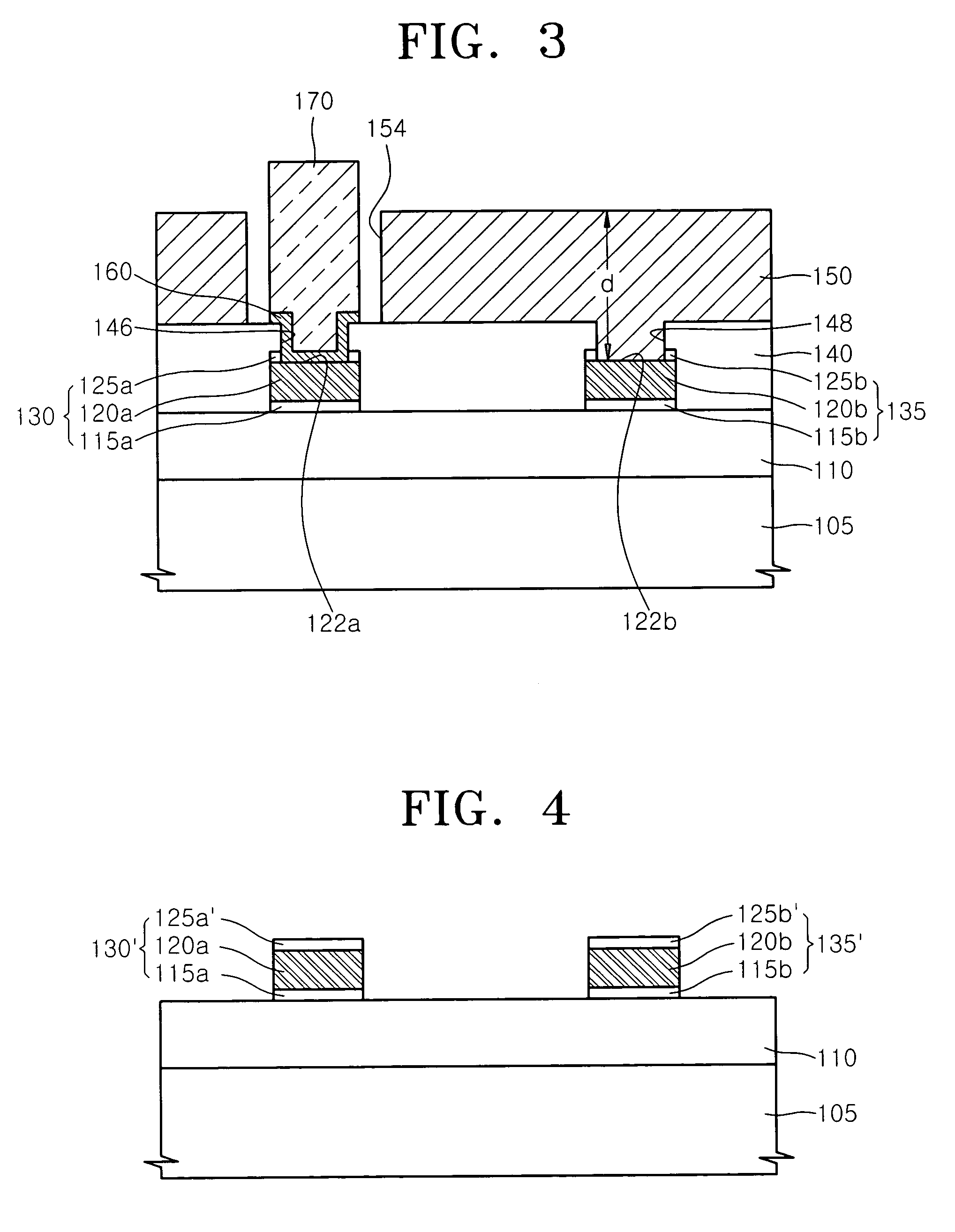
[0027]FIG. 2 is a plan view illustrating a semiconductor device according to an exemplary embodiment of the present invention, and FIG. 3 is a cross-sectional view of the semiconductor device as taken along the line III-III′ of FIG. 2. The semiconductor device according to the present exemplary embodiment of the invention may include the driving device of a LCD (liquid crystal display) device but is not limited to the driving device. For example, the semiconductor device may include a semiconductor device for a COG (chip on glass) assembly.

[0028]Referring to FIG. 2, the semiconductor device comprises at least one or more align mark layers 135, 136, 13...


PUM


Abstract

A semiconductor device includes a pad electrode layer and an align mark layer, formed on the semiconductor substrate. A passivation layer is formed on the semiconductor substrate and exposes at least a portion of the top of the pad electrode layer and at least a portion of the top of the align mark layer. A light-transmitting protecting layer covers at least a portion of the passivation layer, exposes the top portion of the pad electrode layer exposed from the passivation layer, and covers the portion of the align mark layer exposed from the passivation layer.

Description

CROSS-REFERENCE TO RELATED PATENT APPLICATION[0001]This application claims the benefit of Korean Patent Application No. 10-2005-0111994, filed on Nov. 22, 2005, in the Korean Intellectual Property Office, the disclosure of which is hereby incorporated by reference herein in its entirety.BACKGROUND OF THE INVENTION[0002]1. Technical Field[0003]The present invention relates to a semiconductor device and a method of fabricating the same, and more particularly, to a semiconductor device having an alignment mark used as an alignment key in a packaging operation for semiconductor chips and a method of fabricating the same.[0004]2. Discussion of the Related Art[0005]Semiconductor devices formed on a semiconductor substrate are typically assembled for connection to external devices and also packaged to protect these semiconductor devices from the external environment. In particular, a semiconductor device may have a pad electrode layer used as an input / output terminal for being connected to...

Claims


Application Information

Patent Timeline
Patent Type & Authority Patents(United States)
IPC IPC(8): H01L23/544
CPCH01L23/544H01L24/03H01L24/11H01L24/12H01L24/81H01L2223/54426H01L2223/54473H01L2223/5448H01L2224/03912H01L2224/0401H01L2224/1147H01L2224/11474H01L2224/13021H01L2224/13099H01L2224/13144H01L2224/16H01L2224/81121H01L2224/81801H01L2924/01004H01L2924/01005H01L2924/01013H01L2924/01014H01L2924/01022H01L2924/01028H01L2924/01029H01L2924/01033H01L2924/01073H01L2924/01078H01L2924/01079H01L2924/01082H01L2924/014H01L2924/04941H01L2924/04953H01L2924/05042H01L2924/19041H01L2924/19043H01L2924/01006Y10S438/975H01L2224/05556H01L2224/05572H01L2924/00012H01L2924/00014H01L23/12
Inventor HWANG, HO-IKLEE, SOO-CHEOL
Owner SAMSUNG ELECTRONICS CO LTD
Why Eureka
Try Eureka