

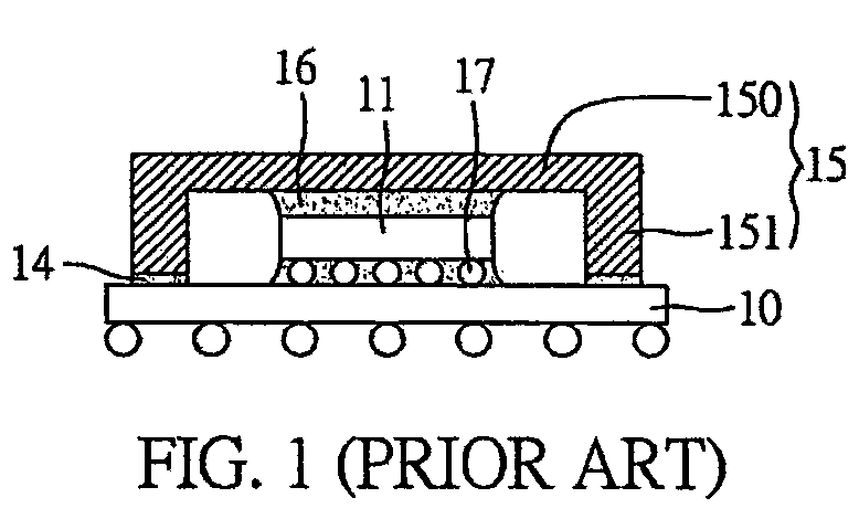
Semiconductor device package with a heat sink and method for fabricating the same
a technology of semiconductor devices and heat sinks, which is applied in the direction of semiconductor devices, semiconductor/solid-state device details, electrical apparatus, etc., can solve the problems of uneven heat sinks, low young's modulus adhesives that fail to provide sufficient support strength to heat sinks, and adversely affect the quality of electrical connection between semiconductor chips and substrates, so as to reduce warpage and control the flatness of heat sinks
- Summary
- Abstract
- Description
- Claims
- Application Information
AI Technical Summary
Benefits of technology
Problems solved by technology
Method used
Image

Examples
Embodiment Construction
[0021]The following illustrative embodiments are provided to illustrate the disclosure of the present invention, these and other advantages and effects can be apparent to those skilled in the art after reading the disclosure of this specification. The present invention can also be performed or applied by other different embodiments. The details of the specification may be on the basis of different points and applications, and numerous modifications and variations can be devised without departing from the spirit of the present invention.
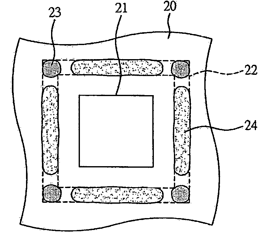
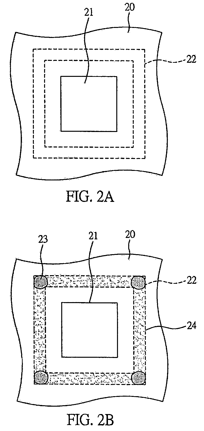
[0022]Referring to FIGS. 2A to 2D, a semiconductor package with a heat sink and a fabrication method thereof according to the present invention are shown.
[0023]Referring to FIG. 2A, a substrate 20 having a heat sink mounting area 22 (marked with dash lines) is provided. A semiconductor chip 21 is flip-chip mounted on the substrate 20 and electrically connected to the substrate 20 via conductive bumps.
[0024]Referring to FIG. 2B, a first adhesive 23 is ...
PUM
 Abstract
Description
Claims
Application Information