Method to form electrostatic discharge protection on flexible circuits using a diamond-like carbon material

a flexible circuit and diamond-like carbon technology, applied in circuit electrostatic discharge protection, integrated arm assemblies, instruments, etc., can solve the problems of esd damage to the thin film head element, signal is susceptible to static noise distortion, over-all hdd cost margin, etc., to prevent esd and circuit noise, esd damage, and a wider range of applicability

Active Publication Date: 2009-02-10
MAGNECOMP
View PDF69 Cites 6 Cited by
  • Summary
  • Abstract
  • Description
  • Claims
  • Application Information

AI Technical Summary

Benefits of technology

[0006]According to the present invention, techniques for preventing ESD and circuit noise are provided. More particularly, the present invention provides a method to prevent ESD damage during the assembly of a HDD. The coating mainly involves an ion-deposition process, for example, filtered cathodic vacuum arc (FCVA). Merely by way of example, the present invention is implemented by using FCVA with a dissipative carbon base thin film coating on a flexible circuit to drain the potential electrostatic charges during circuit assembly and interconnect processes, yet it would be recognized that the invention could use other ion-deposition processes (for example, sputtering, single or dual ion beam, laser ablation, etc.) and have a much broader range of applicability on any electronic apparatus that is susceptible to electrostatic damage and static noise.
[0007]In a specific embodiment, low cost and robust carbon base film coating (for example, tetrahedral amorphous carbon (TAC)) is used for circuit ESD protection. TAC is conventionally used as a machine tool and die coating to improve surface wear resistance. However, TAC can be formulated to exhibit resistivity in the order of 108 to 10−2 ohms. For circuit electrostatic dissipation, a TAC film is formulated to about 106 to 108 ohms as electrically dissipative material and coated on circuit surface. Film deposition can be implemented by FCVA or another ion-deposition process.
[0008]In an alternative embodiment, a robust connection to ground for noise reduction is provided. TAC can be formulated to have low resistance (or its lowest resistance) for use as a ground connection (or a grounding feature), thereby providing good conductivity to ground. Besides TAC, the ground connection can also be formed by other metallic materials by using the same deposition process used for the dissipative film coating or another deposition process.
[0009]The FCVA technique provides ion deposition without the cost of using noble gases and the resulting TAC film exhibits high density and excellent surface wear resistance. The film thickness can be controlled in the range of a nanometer to micrometers. The film thickness, in an embodiment of the invention, can be 1 nm, 5 nm, 10 nm, or greater. The coating area can be selective, by applying either a rigid (or flexible metallic) mask or solvent removable / wet etchable polyimide.
[0022]12. Allow low cost mask material, such as stainless steel.

Problems solved by technology

Production yield of this assembly is critical for overall HDD cost margin.
Yet, this thin film head element is susceptible to low voltage ESD damage, and the signal is susceptible to static noise distortion.
However, these tactics have disadvantages.
For example, due to the natural properties of the polymer film, the resistance and thickness uniformity of the polymer film are hard to control.
Furthermore, the polymer film suffers from environmental attack (e.g., temperature, humidity, etc.) and requires curing time.
With respect to techniques of grounding the slider, they have the disadvantage of high cost due to forming the grounding feature on circuit by sputtering and / or deep-hole plating followed by nickel (Ni) and gold (Au) plating.

Method used


Image

  • Method to form electrostatic discharge protection on flexible circuits using a diamond-like carbon material
  • Method to form electrostatic discharge protection on flexible circuits using a diamond-like carbon material
  • Method to form electrostatic discharge protection on flexible circuits using a diamond-like carbon material

Examples


Embodiment Construction

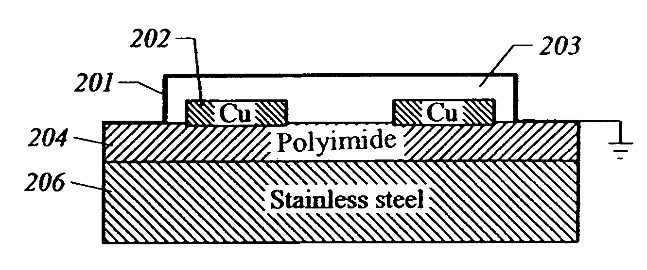
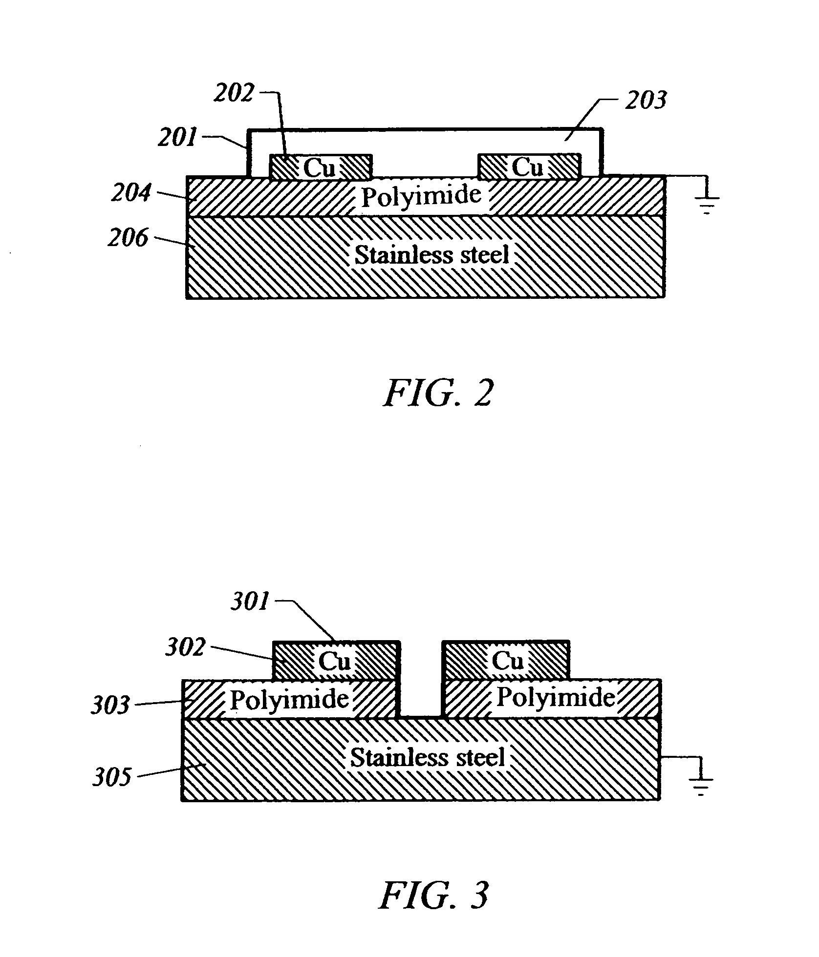
[0053]According to the present invention, techniques for preventing ESD and circuit noise are provided. More particularly, the present invention prevents ESD damage during the assembly of HDD. As an embodiment according to the present invention, a dissipative carbon base thin film is coated on a flexible circuit to drain the potential electrostatic charges during circuit assembly and interconnect processes. The coating is formed by using a FCVA process. Yet, it would be recognized that the invention could use other ion-deposition processes and have a much broader range of applicability on any electronic apparatus that are susceptible to electrostatic damage and static noise.

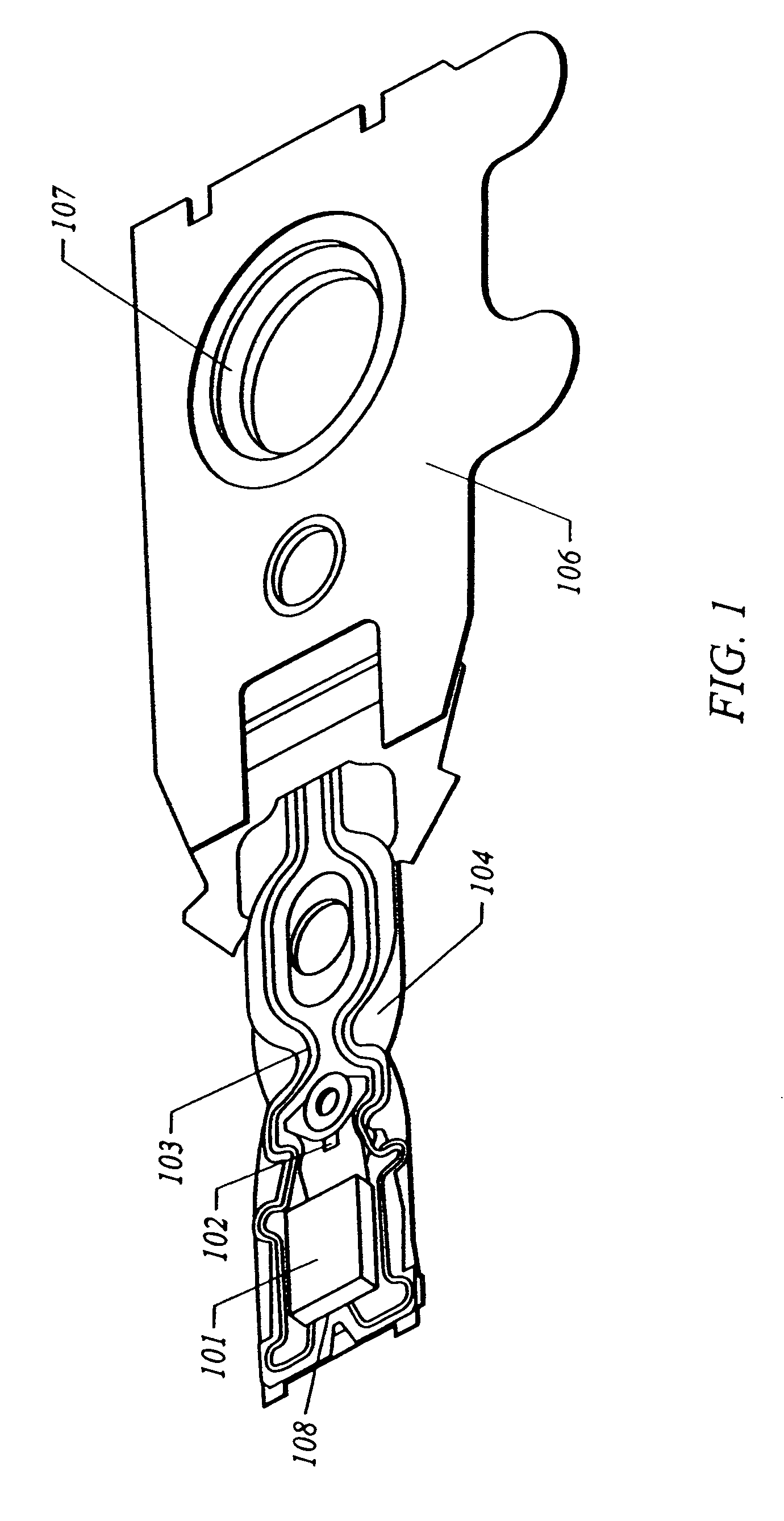
[0054]FIG. 1 is a head gimbal assembly (HGA) top-view diagram. As shown, the apparatus includes a MR head 108 on a slider 101 and is bonded on gimbal 102 by adhesives. The interconnect is formed by connecting the MR head 108 to a flexible circuit 103. This flexible circuit is then routed on a suspension load beam...


PUM

PropertyMeasurementUnit
pressureaaaaaaaaaa
peak energyaaaaaaaaaa
resistanceaaaaaaaaaa

Abstract

Techniques for preventing electrostatic discharge (ESD) and circuit noise are provided. More particularly, the present invention provides a method to prevent ESD damage during the assembly of computer disk commonly called a hard disk for memory applications. The coating mainly involves a ion-deposition process. Merely by way of example, the present invention is implemented by using filtered cathodic vacuum arc (FCVA) with a dissipative crystalline and / or amorphous carbon base thin film coating on a flexible circuit to drain the potential electrostatic charges during circuit assembly and interconnect processes, yet it would be recognized that the invention has a much broader range of applicability on any electronic apparatus that is susceptible to electrostatic damage and static noise.

Description

CROSS-REFERENCES TO RELATED APPLICATIONS[0001]This application claims priority from U.S. provisional patent application No. 60 / 526,164, filed Dec. 1, 2003, entitled “Method for Electro Static Discharge Protection and Noise Reduction of Flexible Circuit by Applying Carbon Base Coating,” and U.S. provisional patent application No. 60 / 538,798, filed Jan. 23, 2004, entitled “Method to Form Electrostatic Discharge Protection on Flexible Circuits,” which disclosures are incorporated herein by reference.BACKGROUND OF THE INVENTION[0002]This invention generally relates to techniques for forming electrostatic discharge (ESD) protection for a computer disk, commonly called a hard disk drive (HDD), throughout its assembly process. More particularly, the present invention provides robust methods and dry processes for preventing electrostatic discharge and circuit noise induced by circuit handling during HDD assembly. Merely by way of example, the present invention is implemented using such meth...

Claims


Application Information

Patent Timeline
Patent Type & Authority Patents(United States)
IPC IPC(8): H05F3/02G11B5/48G11B33/14H02B1/00H05K1/00H05K1/02H05K1/05H05K3/28
CPCG11B5/486G11B33/1493H05K1/0259H05K1/0393H05K1/056H05K3/28H05K2201/0317H05K2201/0323G11B5/40G11B5/484
Inventor THAVEEPRUNGSRIPORN, VISITHU, SZU-HAN
Owner MAGNECOMP
Why Eureka
Try Eureka