Light-emitting device, method for making the same, and electronic apparatus

a light-emitting device and light-emitting technology, applied in the field of light-emitting devices, can solve the problems of insufficient control of voltage drop of the second electrode, and it is more difficult to increase the aperture ratio and sufficiently control the voltage drop. , to achieve the effect of high mechanical strength

Active Publication Date: 2009-02-17
ELEMENT CAPITAL COMMERCIAL CO PTE LTD
View PDF3 Cites 19 Cited by
  • Summary
  • Abstract
  • Description
  • Claims
  • Application Information

AI Technical Summary

Benefits of technology

[0010]Since the auxiliary interconnect is not formed in the gap between the second element group and the third element group, the area of the region where the auxiliary interconnect is formed and the area of the margin region are small compared to the case where every gap between the element groups is provided with the auxiliary interconnect. Therefore, it is easy to achieve both high aperture ratio and low resistance auxiliary interconnect. For example, it is possible to increase the aperture ratio without reducing the width of the auxiliary interconnect or to increase the width (to reduce the resistance) of the auxiliary interconnect without reducing the aperture ratio.
[0021]The mask used in the above method has no opening in a region corresponding to a gap between the second element group and the third element group. Therefore, the mask has high mechanical strength compared to a mask that has openings corresponding to all gaps between the element groups. Therefore, errors in the auxiliary interconnect due no deformation (bending) of the mask and breakage of the mask can be controlled.

Problems solved by technology

In this case, however, due to the increase in resistance value of the auxiliary interconnects, the voltage drop of the second electrode cannot be sufficiently controlled.
Since neither auxiliary interconnect nor light-emitting element is formed in the margin region, it is more difficult both to increase the aperture ratio and to sufficiently control the voltage drop.

Method used


Image

  • Light-emitting device, method for making the same, and electronic apparatus
  • Light-emitting device, method for making the same, and electronic apparatus
  • Light-emitting device, method for making the same, and electronic apparatus

Examples


first exemplary embodiment

A: First Exemplary Embodiment

Configuration of Light-Emitting Device

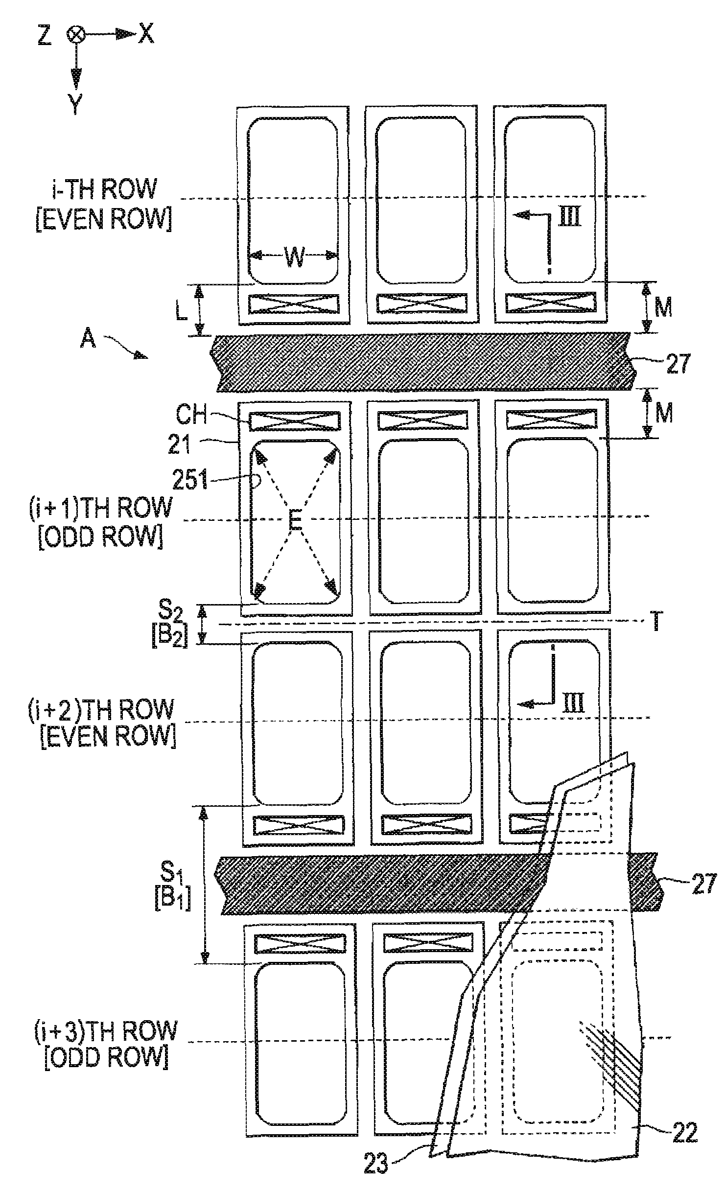
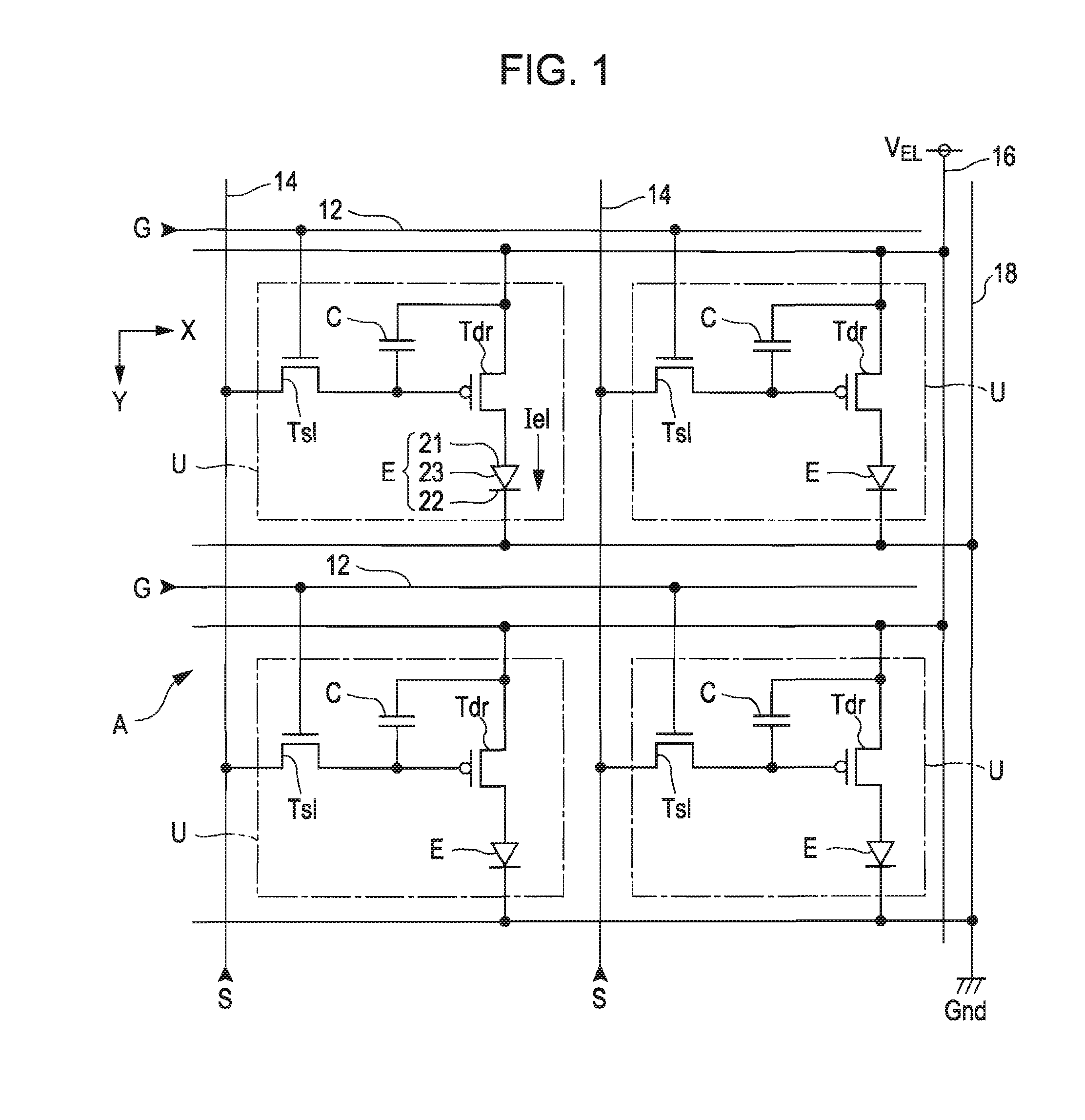
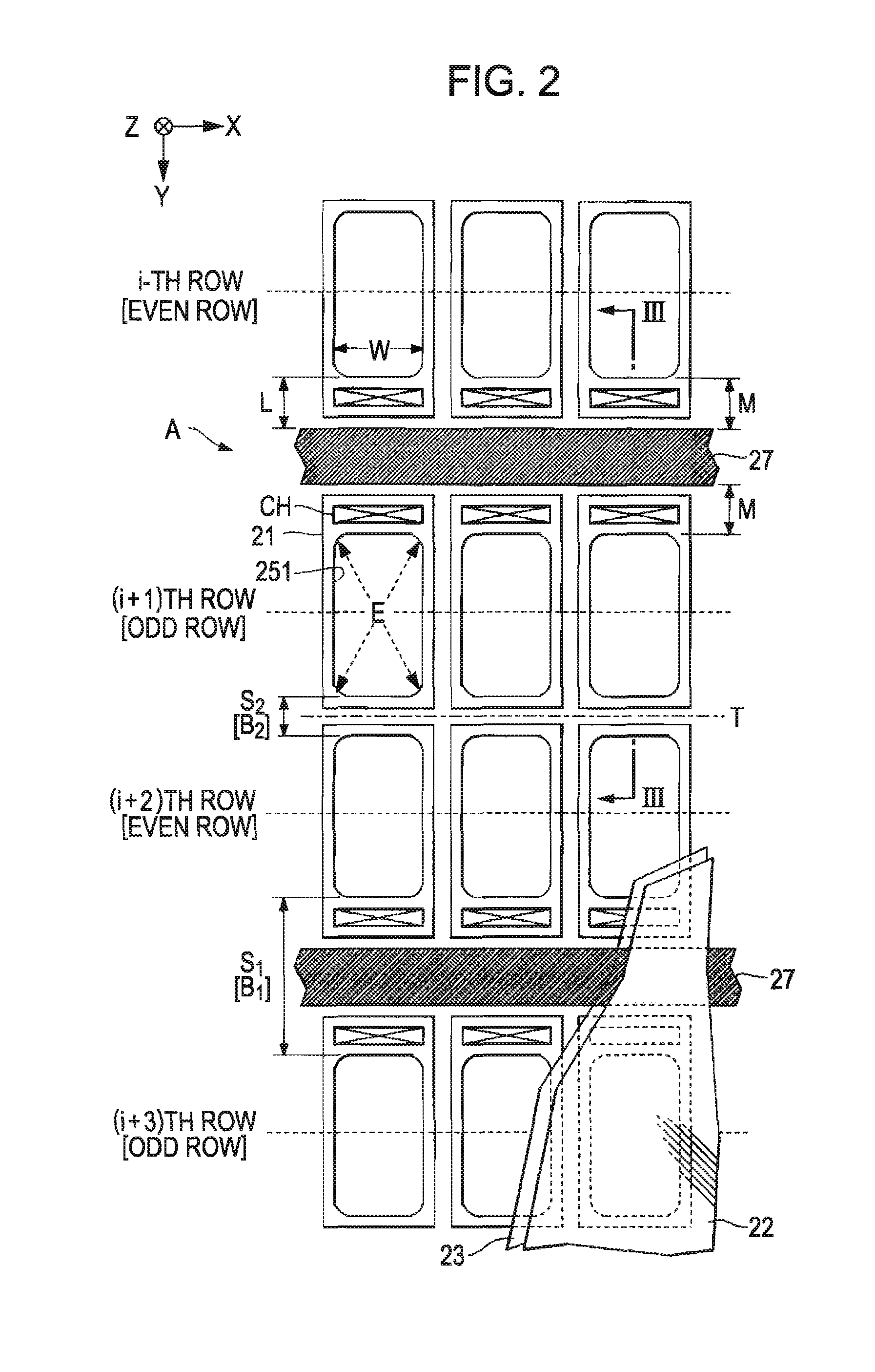
[0033]FIG. 1 is a circuit diagram showing the electrical configuration of a light-emitting device according to an exemplary embodiment of the invention. The light-emitting device has an element array portion A in which a plurality of unit circuits (pixel circuits) U are arranged. In the element array portion A are formed a plurality of scanning lines 12 extending in the X direction and a plurality of data lines 14 extending in the Y direction perpendicular to the X direction. The unit circuits U are disposed at positions corresponding to the intersections of the scanning lines 12 and the data lines 14. Therefore, the plurality of unit circuits U are arranged in the X direction and the Y direction in a matrix.

[0034]One unit circuit U Includes a drive transistor Tdr and a light-emitting element E disposed on a route from a source line 16 (source voltage VEL) to a ground line 18 (ground voltage Gnd). The light-emitting ...

second exemplary embodiment

B: Second Exemplary Embodiment

[0058]Next, a second exemplary embodiment of the invention will be described. In the description of this exemplary embodiment, the same reference numerals will be used to designate the same components as those in the first exemplary embodiment, so that the detailed description will be omitted.

[0059]FIG. 5 is a plan view showing the configuration of the element array portion A according to the exemplary embodiment (a plan view corresponding to FIG. 2). In the first exemplary embodiment, the auxiliary interconnects 27 extend along the short side of the light-emitting elements E (in the X direction). In contrast, in the exemplary embodiments the auxiliary interconnects 27 extend along the long side of the light-emitting elements E (in the Y direction) as shown in FIG. 5. FIG. 5 shows three rows of light-emitting elements E belonging to the j-th to (j+3)th columns. The j-th column and the (j+2)th column are even columns, and the (j+1)th column and the (j+3)...

third exemplary embodiment

C: Third Exemplary Embodiment

[0063]Next, a third exemplary embodiment of the invention will be described. In the description of this exemplary embodiment, the same reference numerals will be used to designate the same components as those in the first exemplary embodiment, so that the detailed description will be omitted.

[0064]FIG. 6 is a plan view showing the configuration of the element array portion A according to the exemplary embodiment (a plan view corresponding to FIG. 2). FIG. 7 is a sectional view taken along line VII-VII of FIG. 6. In the first exemplary embodiment, the auxiliary interconnects 27 do note overlap with the contact holes CH. In contrast, in the exemplary embodiment, as shown in FIGS. 6 and 7, the auxiliary interconnects 27 overlap with the contact holes CH as viewed from the Z direction. That is to say, the auxiliary interconnects 27 have a width substantially equal to the width of the partition layer 25, and overlap with the contact holes CH corresponding to ...


PUM


Abstract

A light-emitting device includes an element array portion and an auxiliary interconnect. The element array portion includes a plurality of element groups. Each element group includes a plurality of light-emitting elements arranged in a first direction. Each light-emitting element has a structure such that a light-emitting layer lies between a first electrode and a second electrode. The element groups are arranged in a second direction perpendicular to the first direction. The auxiliary interconnect is formed of a material having a resistivity lower than the resistivity of the second electrode and is electrically connected to the second electrode of each light-emitting element. The plurality of element groups include a first element group and a second element group adjacent to each other and a third element group adjacent to the opposite side of the second element group from the first element group. The auxiliary interconnect extends in the first direction in a gap between the first element group and the second element group but is not formed in a gap between the second element group and the third element group.

Description

[0001]The entire disclosure of Japanese Application No. 2006-088306, filed Mar. 28, 2006 is expressly incorporated by reference herein.BACKGROUND[0002]1. Technical Field[0003]The present invention relates to the structure of a light-emitting device that employs a light-emitting element such as an organic light-emitting diode element.[0004]2. Related Art[0005]A light-emitting device in which a large number of light-emitting elements are arranged in a matrix has been proposed. Each light-emitting element includes a first electrode, a second electrode, and a light-emitting layer lying between both electrodes. JP-A-2002-352963 discloses a top emission light-emitting device that includes a light-transmissive conductive layer shared by a plurality of light-emitting elements as their common second electrode. The device further includes auxiliary interconnects formed in the gaps between the light-emitting elements. The auxiliary interconnects are formed of a material having a resistivity lo...

Claims


Application Information

Patent Timeline
Patent Type & Authority Patents(United States)
IPC IPC(8): H01L29/18
CPCH01L51/5234H01L27/3246H01L2251/5315H10K59/122H10K50/828H10K2102/3026H05B33/26
Inventor KUBOTA, TAKEHIKO
Owner ELEMENT CAPITAL COMMERCIAL CO PTE LTD
Why Eureka
Try Eureka