Display device having an anisotropic-conductive adhesive film

a technology of anisotropic conductive and adhesive film, which is applied in the direction of optics, printed circuit aspects, instruments, etc., can solve the problems of short-circuit failure, short-circuit failure between adjacent terminals, corrosion of exposed wires, etc., and achieve the effect of suppressing short-circuit failur

Active Publication Date: 2009-02-17
ROVI TECH CORP
View PDF7 Cites 14 Cited by
  • Summary
  • Abstract
  • Description
  • Claims
  • Application Information

AI Technical Summary

Benefits of technology

[0014]In view of the above problems in the conventional technique, it is an object of the present invention to provide a display device capable of suppressing a short-circuit failure between adjacent terminals.
[0016]In accordance with the present invention, the insulating property of the exposed surface of the first particles in the conductive particles prevents a short-circuit failure between adjacent terminals caused by alignment of the conductive particles in contact with one another, while assuring electric contact between the first terminals and the second terminals after thermal compression of the ACF.

Problems solved by technology

The alignment of the conductive particles 32 in contact with one another will cause a short-circuit failure between adjacent terminals.
The sufficient distance D3, however, may allow a foreign object or foreign particle to be attached onto the exposed wires or may cause corrosion of the exposed wires 22 in the flexible wiring member 20.
This may also cause a short-circuit failure.
For avoiding the short-circuit failure between adjacent terminals, another insulating film may be formed on the exposed terminals 24; however, it increases the process steps and raises the cost of the LCD device.
However, reduction of the pitch of the terminals in the current semiconductor devices makes it difficult to employ the configuration of the overcoat film having the protrusion in the space between adjacent terminals while exposing the terminals.

Method used


Image

  • Display device having an anisotropic-conductive adhesive film
  • Display device having an anisotropic-conductive adhesive film
  • Display device having an anisotropic-conductive adhesive film

Examples


first embodiment

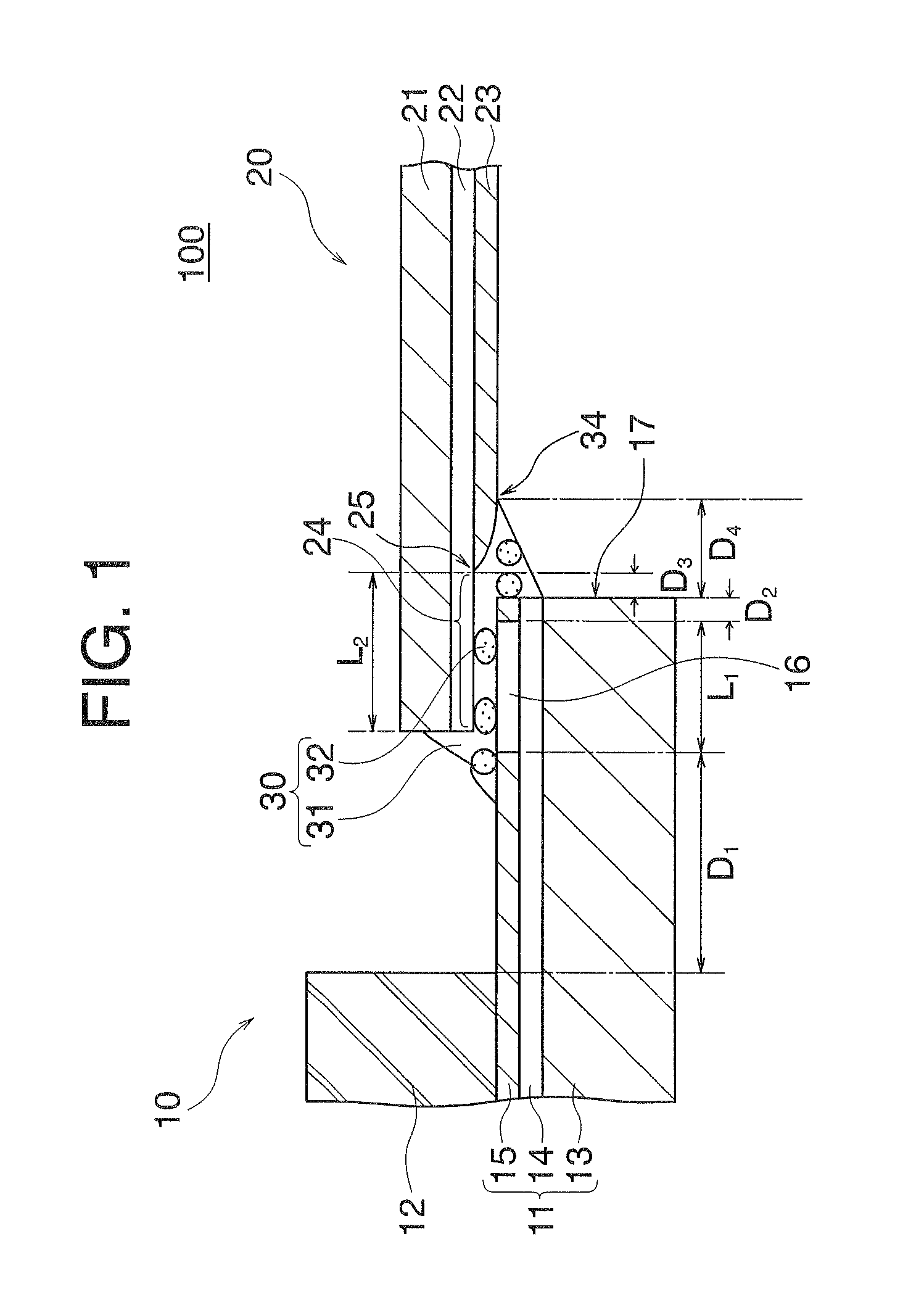
[0040]FIG. 1 shows an edge portion of a display device (LCD device) according to the present invention. The LCD device, generally designated by numeral 100, includes an active-matrix LCD panel 10, and a plurality of flexible wiring members 20 each used as a wiring substrate for mounting a driver IC driving the LCD panel 10.

[0041]The LCD panel 10 includes an active-matrix substrate 11, a color-filter substrate 12 opposing the active-matrix substrate 11, and a LC layer (not shown) sandwiched between the active-matrix substrate 11 and the color-filter substrate 12. The active-matrix substrate 11 includes a plurality active devices, such as TFTs each disposed for controlling one of an array of pixels. The color-filter substrate 12 includes color filters each for one of the pixels.

[0042]The active-matrix substrate 11 includes a glass substrate body 13, on which a plurality of conductive leads (leads) 14 are formed to connect to TFTs. The leads 14 extend normal to the extending direction ...

second embodiment

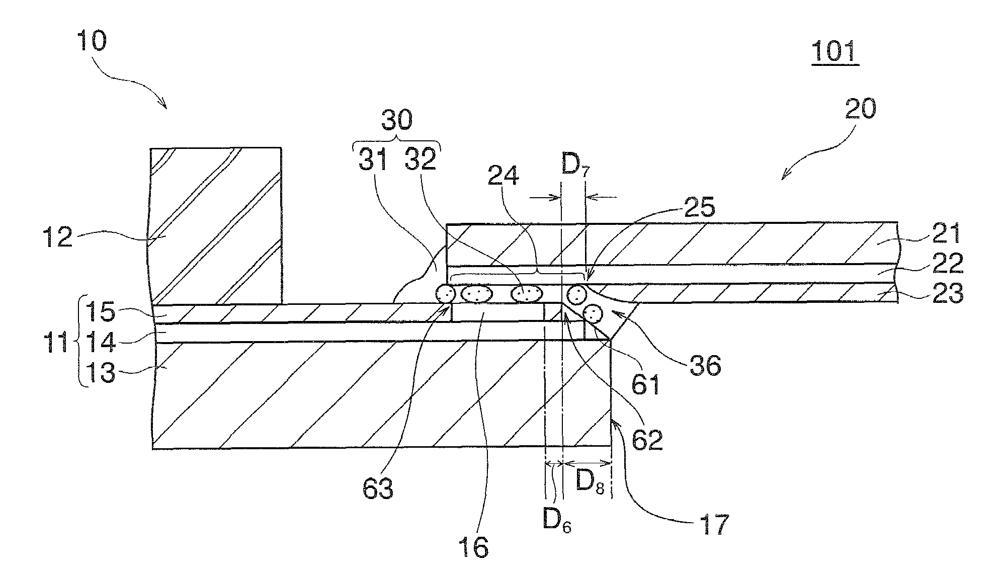
[0066]FIG. 10 shows a LCD device according to the present invention. The LCD device, generally designated by numeral 101, has a chamfer 61 formed on the edge portion of the active-matrix substrate 11 onto which the flexible wiring member 20 is fixed. For example, the distance (D6) between the proximal edge 62 of the chamfer 61 and the terminals 16 is 0.3 mm, the distance (D7) between the proximal edge 62 of the chamfer 61 and the distal edge 25 of the overcoat film 23 is 0.1 mm, and the distance (D8) between the width of the chamfer 61 as measured parallel to the surface of the substrates (substrate surface) is 0.3 mm. The surface of the chamfer 61 is at 30 degrees away from the substrate surface, for example.

[0067]The ACF 30 covers the entire terminals 24 of the flexible wiring member 20 and a portion of the overcoat film 23, and extends toward the edge 17 of the active-matrix substrate 11, after the thermal compression process. The LCD device 101 is similar to the LCD device 100 o...

third embodiment

[0071]FIG. 11 shows a LCD device according to the present invention. The LCD device, generally designated by numeral 102, includes exposed leads 14 which configure terminals 64 at the end thereof. The ACF 30 covers the exposed leads 14 in the area between the edge of the color-filter substrate 12 and the edge 17 of the active-matrix substrate 11. The LCD device 102 is similar to the LCD device 100 of FIG. 1 except for these configurations.

[0072]In manufacture of the LCD device 102, the end portion of the leads 14 are not covered with an insulating film, and the end portion of the leads 14 configure terminals 64 without using an additional treatment of the leads 14. The ACF 30 is bonded onto the active-matrix substrate 11 between the edge of the color-filter substrate 12 and the edge 17 of the active-matrix substrate 11.

[0073]The process for manufacturing the LCD device 102 of the present embodiment obviates the steps of forming an insulating film on the leads 14 and configuring the ...


PUM

PropertyMeasurementUnit
areaaaaaaaaaaa
distance D2aaaaaaaaaa

Abstract

A liquid crystal display (LCD) device includes a LCD panel and a flexible wiring member coupled together by an anisotropic-conductive adhesive film (ACF). The ACF includes insulating resin and a plurality of conductive particles dispersed therein and each having an insulating film on a conductive body. The insulating film is broken by the thermal compression of the ACF during manufacture of the LCD device, thereby allowing terminals of the LCD panel and terminals of the flexible wiring member to be electrically coupled together.

Description

BACKGROUND OF THE INVENTION[0001](a) Field of the Invention[0002]The present invention relates to a display device having an anisotropic-conductive adhesive film and, more particularly, to a display device including a display panel and a flexible wiring member bonded onto the display panel by using an anisotropic-conductive adhesive film.[0003](b) Description of the Related Art[0004]Display devices, such as a LCD device, include a display panel and a drive unit including a driver IC electrically coupled to the display panel for driving the display panel. The drive unit includes a flexible wiring substrate or flexible wiring member, on which the driver IC is mounted using a tape-automated-bonding (TAB) technique. The flexible wiring member, on which the driver IC is fixed, is coupled at an end thereof onto an edge portion of the display panel, and is folded onto the rear surface of the display panel for mounting the driver IC on the rear side of the display panel. This configuration ...

Claims


Application Information

Patent Timeline
Patent Type & Authority Patents(United States)
IPC IPC(8): G02F1/1345
CPCG02F1/13452H01L24/83H05K3/323H05K3/361H01L24/29H01L2924/07811H01L2224/2939H01L2224/29355H01L2224/2929H01L2224/81903H01L2924/014H01L2924/01006H01L2224/29399H01L2224/838H01L2924/01029H01L2924/01033H01L2924/01049H01L2924/0105H01L2924/01078H01L2924/01079H01L2924/01082H01L2924/0781H01L2924/14H05K2201/0224H05K2203/0278H01L2224/13016H01L2224/83851H01L2924/00014H01L2924/00
Inventor KUDO, KIYOFUMINAKANISHI, FUTOSHI
Owner ROVI TECH CORP
Why Eureka
Try Eureka